M59DR016 查看數據表(PDF) - STMicroelectronics
零件编号
产品描述 (功能)
生产厂家
M59DR016 Datasheet PDF : 37 Pages
| |||
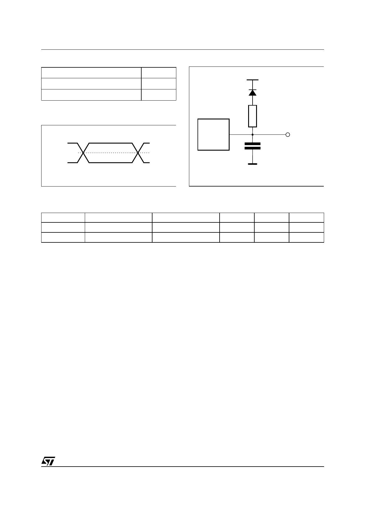
Table 22. AC Measurement Conditions
Input Rise and Fall Times
≤ 4ns
Input Pulse Voltages
0 to VDDQ
Input and Output Timing Ref. Voltages
VDDQ/2
Figure 3. Testing Input/Output Waveforms
VDDQ
0V
VDDQ/2
AI02315
M59DR016C, M59DR016D
Figure 4. AC Testing Load Circuit
VDDQ / 2
1N914
DEVICE
UNDER
TEST
3.3kΩ
OUT
CL = 30pF
CL includes JIG capacitance
AI02316
Table 23. Capacitance (1)
(TA = 25 °C, f = 1 MHz)
Symbol
Parameter
CIN
Input Capacitance
COUT
Output Capacitance
Note: 1. Sampled only, not 100% tested.
Test Condition
VIN = 0V
VOUT = 0V
Min
Max
Unit
6
pF
12
pF
19/37
Share Link: 