UAA3580 查看數據表(PDF) - Philips Electronics
零件编号
产品描述 (功能)
生产厂家
UAA3580
Philips Electronics

UAA3580 Datasheet PDF : 24 Pages
| |||
Philips Semiconductors
Wideband code division multiple access
frequency division duplex zero IF receiver
Objective specification
UAA3580
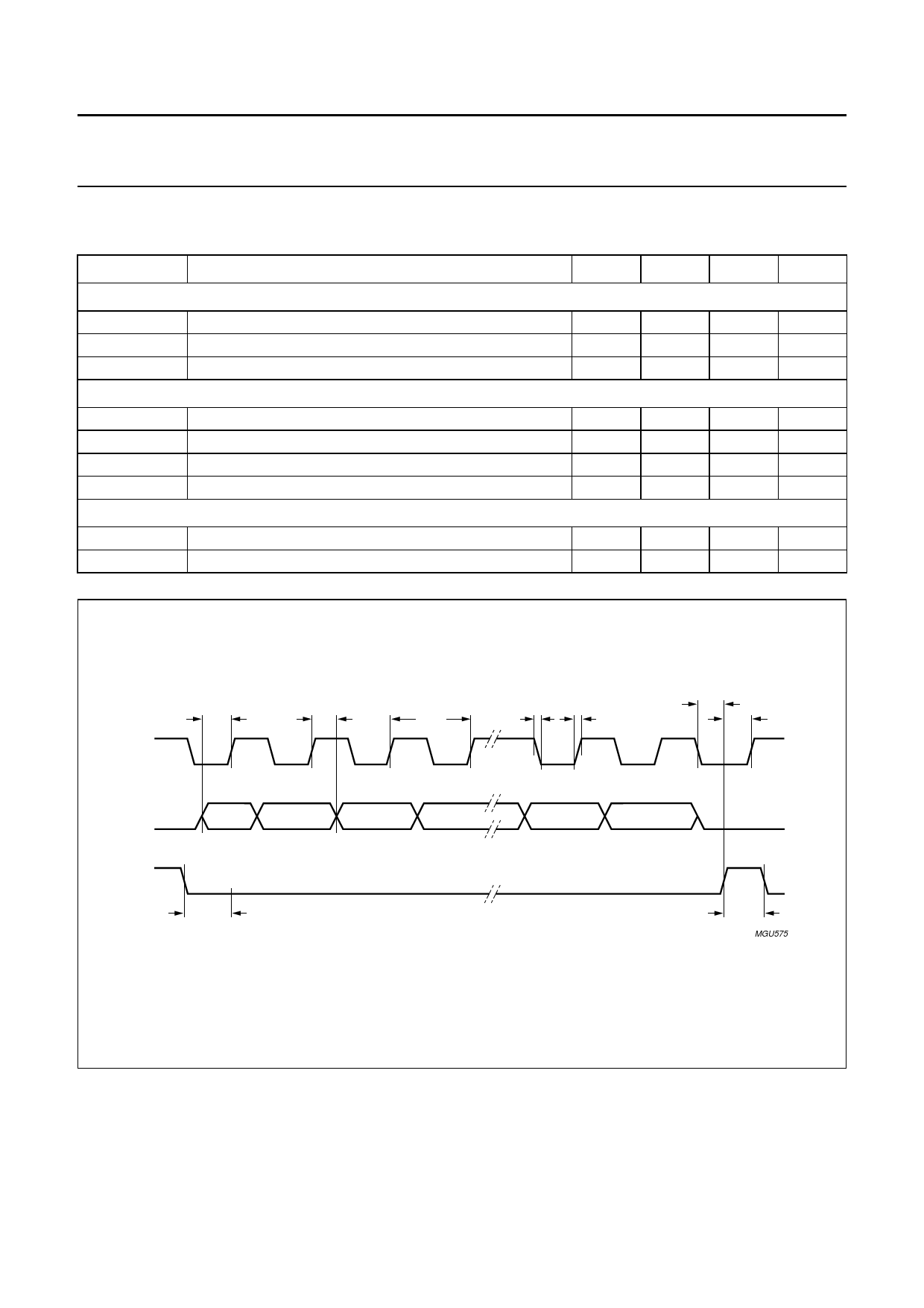
15 SERIAL BUS TIMING CHARACTERISTICS
VCCA = 2.6 V; VCCA(CP) = 2.6 V; VDDD = 1.6 V; Tamb = 25 °C; unless otherwise specified.
SYMBOL
PARAMETER
MIN.
TYP.
Serial clock; pin CLK
ti(r)
input rise time
ti(f)
input fall time
Tcyc
clock period
Enable; pin EN
−
−
−
−
67
−
td(START)
delay to rising clock edge
td(END)
delay from last falling clock edge
tW
minimum inactive pulse width
tsu;EN
enable set-up time to next clock
Register serial input data; pin DATA
200
−
100
−
400
−
200
−
tsu;DATA
th;DATA
input data to clock set-up time
input data to clock hold time
25
−
25
−
MAX.
20
20
−
−
−
−
−
−
−
UNIT
ns
ns
ns
ns
ns
ns
ns
ns
ns
handbook, full pagewidth tsu;DAT
CLK
DATA
MSB
EN
td(START)
th;DAT
Tcyc
ti(f) ti(r)
td(END)
tsu;EN
LSB
ADDRESS
tW
MGU575
Fig.3 Serial bus timing diagram.
2002 Oct 30
18
Share Link: