UPD75064GBA-XXX-3B4 查看數據表(PDF) - NEC => Renesas Technology
零件编号
产品描述 (功能)
生产厂家
UPD75064GBA-XXX-3B4 Datasheet PDF : 68 Pages
| |||
µPD75064, 75066, 75068, 75064(A), 75066(A), 75068(A)
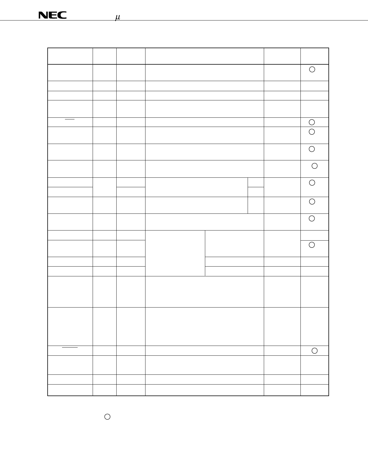
3.2 Non-Port Pins
Pin name
TI0
PTO0
PCL
BUZ
SCK
SO/SB0
SI/SB1
INT4
INT0
INT1
INT2
KR0 - KR3
AN0 - AN3
AN4 - AN7
AVREF
AVSS
X1, X2
XT1, XT2
RESET
IC
VDD
VSS
Input/
output
Shared
with
Function
When reset
Input
P13
Input for receiving external event pulse signal for
–
timer/event counter
I/O
P20
Timer/event counter output
Input
I/O
P22
Clock output
Input
I/O
P23
Output frequency selectable
(for buzzer output or system clock trimming)
Input
I/O
P01
Serial clock I/O
Input
I/O
P02
Serial data output
Serial bus I/O
Input
I/O
P03
Serial data input
Serial bus I/O
Input
Input
P00
Edge-detective vectored interrupt input
–
(both rising and falling edges enabled)
Input
P10
Edge-detective vectored interrupt input Note 2
–
P11
(detection edge selectable)
Note 3
Input
P12
Edge-detective testable input
(rising edge detection)
Note 3
–
I/O P60 - P63/ Parallel falling edge detection testable input
AN4 - AN7
Input
Input P110 - P113 For A /D converter only 8-bit analog input
Input
I/O P60 - P63/
KR0 - KR3
Input
–
Reference voltage input
–
–
–
GND potential
–
Input
–
Crystal/ceramic connection for main system clock
–
generation. When external clock signal is used,
the signal should be applied to X1, and its reverse
phase signal to X2.
Input
–
Crystal connection for subsystem clock genera-
–
tion. When external clock signal is used, the
signal should be applied to XT1, and its reverse
phase signal to XT2. XT1 can be used as a 1-bit
input (test).
Input
–
System reset input
–
–
–
Internally connected.
–
(Connect this pin directly to VDD)
–
–
Positive power supply
–
–
–
GND potential
–
I/O circuit
typeNote 1
B -C
E-B
E-B
E-B
F -A
F -B
M -C
B
B -C
B -C
Y -D
Y-A
Y -D
Z
Z
–
–
B
–
–
–
Notes 1. The circle ( ) indicates the Schmitt trigger input.
2. Clock synchronous
3. Asynchronous
9
Share Link: 