KSY44 查看數據表(PDF) - Siemens AG
零件编号
产品描述 (功能)
生产厂家
KSY44 Datasheet PDF : 3 Pages
| |||
KSY 44
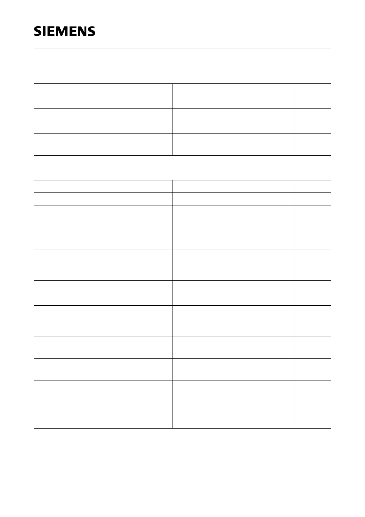
Maximum Ratings
Parameter
Operating temperature
Storage temperature
Supply current
Thermal conductivity
soldered, in air
Symbol
TA
Tstg
I1
GthA
GthC
Characteristics (TA = 25 °C)
Nominal supply current
Open-circuit sensitivity
Open-circuit Hall voltage
I1 = I1N, B = 0.1 T
Ohmic offset voltage
I1 = I1N, B = 0 T
Linearity of Hall voltage
B = 0…0.5 T
B = 0…1.0 T
Input resistance
B=0 T
Output resistance
B=0 T
Temperature coefficient of the
open-circuit Hall voltage
I1 = I1N, B = 0.1 T
Temperature coefficient of the internal
resistance, B = 0 T
Temperature coefficient of ohmic offset
voltage, I1 = I1N, B = 0 T
Inductive zero component, I1N = 0
Switch-on drift of the ohmic offset
voltage I1 = I1N, B = 0 T
Noise figure
I1N
KB0
V20
VR0
FL
R10
R20
TCV20
TCR10, R20
TCVR0
A 1)
2
dV02)
∆V03)
F
Value
– 40…+ 175
– 50…+ 180
10
≥ 1.5
≥ 2.2
7
150…265
105…185
≤ ± 15
≤ ± 0.2
≤ ± 0.7
600…900
1000…1500
∼ – 0.03
∼ + 0.3
∼ – 0.3
0.16
≤ 0.3
≤ 0.1
∼ 10
Unit
°C
°C
mA
mW/K
mW/K
mA
V/AT
mV
mV
%
%
Ω
Ω
%/K
%/K
%/K
cm2
mV
mV
dB
1) With time varying induction there exists an inductive voltage Vind between the Hall voltage terminals (supply
current I1 = 0):
Vind = A2 × dB/dt
×
10-4
with
V(V),
A2
(cm2),
B(T),
t(s)
2) dV0 = V0(t = 1s) – V0(t = 0.1 s)
3) ∆V0 = V0(t = 3m) – V0(t = 1 s)
Semiconductor Group
2
1998-11-13
Share Link: 