MCP1256 查看數據表(PDF) - Microchip Technology
零件编号
产品描述 (功能)
生产厂家
MCP1256
Microchip Technology

MCP1256 Datasheet PDF : 24 Pages
| |||
MCP1256/7/8/9
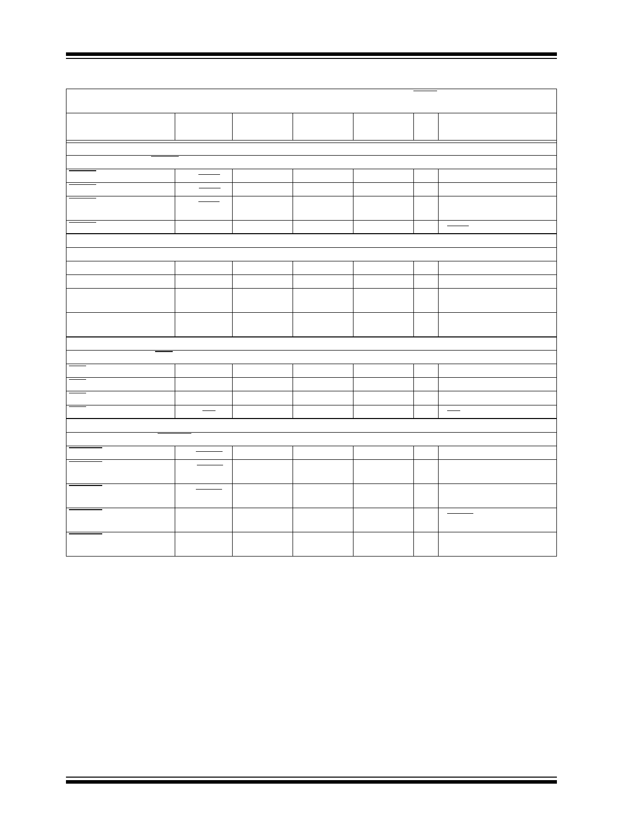
DC CHARACTERISTICS (CONTINUED)
Electrical Specifications: Unless otherwise indicated, all limits apply for VIN = 1.8V to 3.6V, SHDN = VIN, CIN = COUT = 10 μF,
C1 = C2 = 1 μF, IOUT = 10 mA, TJ = -40°C to +125°C. Typical values are at TJ = +25°C.
Parameters
Sym
Min
Typ
Max
Unit
s
Conditions
MCP1256 and MCP1257 Devices
SLEEP Mode Input - SLEEP
SLEEP Input Voltage Low
VIL(SLEEP)
—
SLEEP Input Voltage High VIH(SLEEP)
1.4
SLEEP Input Leakage
ILK(SLEEP)
—
Current
SLEEP Quiescent Current
IQ
—
MCP1256 and MCP1258 Devices
Power-Good Output - PGOOD
PGOOD Threshold
PGOOD Hysteresis
PGOOD Output Low
Voltage
VTH
—
VHYS
—
VOL
—
PGOOD Input Leakage
ILK(PGOOD)
—
Current
MCP1257 and MCP1259
Low-Battery Output - LBO
LBO Threshold
VTH
—
LBO Hysteresis
VHYS
—
LBO Output Low Voltage
VOL
—
LBO Input Leakage Current ILK(LBO)
—
MCP1258 and MCP1259
BYPASS Mode Input - BYPASS
BYPASS Input Voltage Low VIL(BYPASS)
—
BYPASS Input Voltage
VIH(BYPASS)
1.4
High
BYPASS Input Leakage
ILK(BYPASS)
—
Current
BYPASS Quiescent
Current
IQ
—
BYPASS Input-to-Output
RBYPASS
—
Impedance
—
—
0.001
10
93
110
25
0.02
1.95
240
25
0.02
—
—
0.001
0.25
1.5
0.4
V
—
V
0.1
μA
20
μA VSLEEP = 0V, IOUT = 0 mA
—
% Percent of VOUT Falling
—
mV VOUT Rising
100
mV ISINK = 0.5 mA, VIN = 1.8V
1
μA VPGOOD = VIN
—
V VIN Falling
—
mV VIN Rising
100
mV ISINK = 0.5 mA, VIN = 1.8V
1
μA VLBO = VIN
0.4
V
—
V
0.1
μA
2
μA VBYPASS = 0V, IOUT = 0 mA,
TJ = +25°C
—
Ω VIN = 2.4V
DS21989A-page 4
© 2006 Microchip Technology Inc.
Share Link: