AD8221 查看數據表(PDF) - Analog Devices
零件编号
产品描述 (功能)
生产厂家
AD8221 Datasheet PDF : 24 Pages
| |||
AD8221
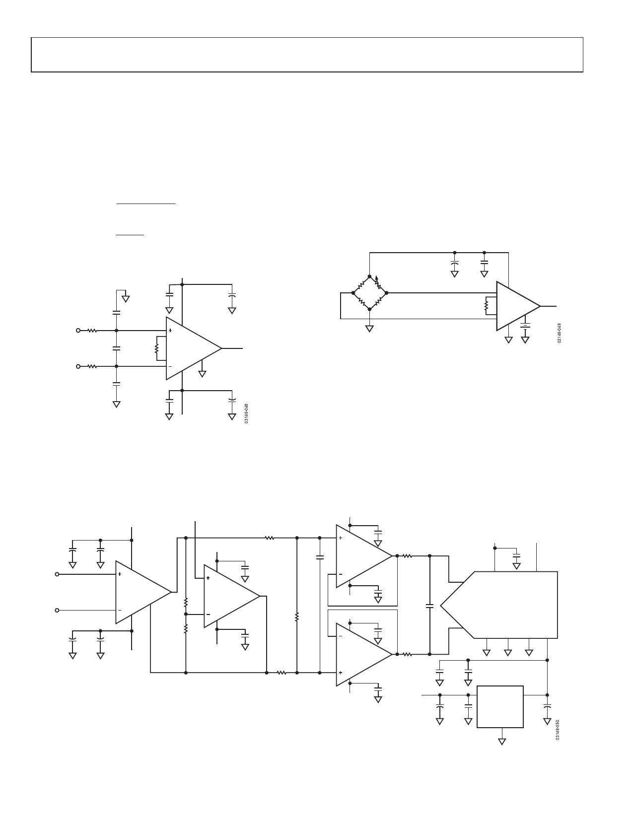
RF INTERFERENCE
RF rectification is often a problem when amplifiers are used in
applications where there are strong RF signals. The disturbance
can appear as a small dc offset voltage. High frequency signals
can be filtered with a low-pass RC network placed at the input
of the instrumentation amplifier, as shown in Figure 49. The
filter limits the input signal bandwidth according to the following
relationship:
CD affects the difference signal, and CC affects the common-
mode signal. Values of R and CC should be chosen to minimize
RFI. Mismatch between the R × CC at the positive input and the
R × CC at the negative input degrades the CMRR of the AD8221.
By using a value of CD one magnitude larger than CC, the effect
of the mismatch is reduced, and therefore, performance is
improved.
PRECISION STRAIN GAGE
FilterFreqDiff
FilterFreqCM
where CD t 10CC.
1
2πR(2CD CC)
1
2πRCC
+15V
0.1µF
10µF
CC
R
4.02k
CD
R
4.02k
CC
1nF
+IN
10nF
R1
499
–IN
AD8221
REF
VOUT
1nF
0.1µF
10µF
–15V
Figure 49. RFI Suppression
The low offset and high CMRR over frequency of the AD8221
make it an excellent candidate for bridge measurements. As
shown in Figure 50, the bridge can be directly connected to
the inputs of the amplifier.
+5V
10µF 0.1µF
350
350
350
350
+IN +
R AD8221
–
–IN
+2.5V
Figure 50. Precision Strain Gage
CONDITIONING ±10 V SIGNALS FOR A +5 V
DIFFERENTIAL INPUT ADC
There is a need in many applications to condition ±10 V signals.
However, many of today’s ADCs and digital ICs operate on
much lower, single-supply voltages. Furthermore, new ADCs
have differential inputs because they provide better common-
mode rejection, noise immunity, and performance at low supply
voltages. Interfacing a ±10 V, single-ended instrumentation
amplifier to a +5 V, differential ADC can be a challenge.
Interfacing the instrumentation amplifier to the ADC requires
attenuation and a level shift. A solution is shown in Figure 51.
+12V
+2.5V
10µF 0.1µF
+IN
10µF
–IN
0.1µF
AD8221
R1
REF 10k
R2
10k
–12V
+12V
0.1µF
OP27
0.1µF
–12V
R3
1k
C1
470pF
R5
499
R4
1k
+12V
0.1µF
AD8022
(½)
0.1µF
–12V
+12V
0.1µF
AD8022
(½)
R6
27.4
C2
220µF
R7
27.4
+5V
+5V
10nF
AVDD
VIN(+)
DVDD
AD7723
VIN(–)
AGND DGND REF1 REF2
220nF 10nF
0.1µF
–12V
+5V
10µF
0.1µF
+VIN
2.5V
VOUT
AD780 22µF
GND
Figure 51. Interfacing to a Differential Input ADC
Rev. C | Page 20 of 24
Share Link: 