Q67100-H3765 ТЪЦуюІТЋИТЊџУАе№╝ѕPDF№╝Ѕ - Siemens AG
жЏХС╗Ху╝ќтЈи
С║ДтЊЂТЈЈУ┐░ (тіЪУЃй)
ућЪС║Дтјѓт«Х
Q67100-H3765 Datasheet PDF : 26 Pages
| |||
SLx 24C64
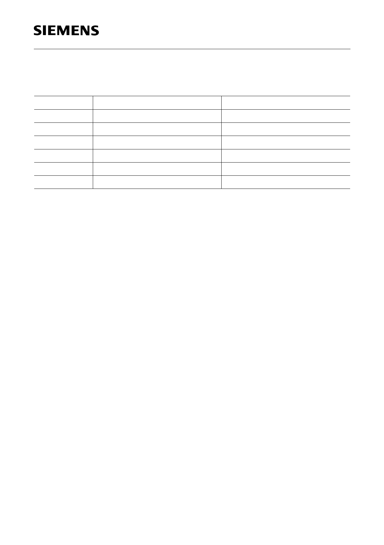
Pin Definitions and Functions
Table 1
Pin No.
Symbol
1, 2, 3
CS0, CS1, CS2
4
VSS
5
SDA
6
SCL
7
WP
8
VCC
Function
Chip select inputs
Ground
Serial bidirectional data bus
Serial clock input
Write protection input
Supply voltage
Pin Description
Serial Clock (SCL)
The SCL input is used to clock data into the device on the rising edge and to clock data
out of the device on the falling edge.
Serial Data (SDA)
SDA is a bidirectional pin used to transfer addresses, data or control information into the
device or to transfer data out of the device. The output is open drain, performing a wired
AND function with any number of other open drain or open collector devices. The SDA
bus requires a pull-up resistor to VCC.
Chip Select (CS0, CS1, CS2)
The CS0, CS1 and CS2 pins are chip select inputs either hard wired or actively driven
to VCC or VSS. These inputs allow the selection of one of eight possible devices sharing
a common bus.
Write Protection (WP)
WP switched to VSS allows normal read/write operations.
WP switched to VCC protects the EEPROM against changes (hardware write protection).
Semiconductor Group
5
Preliminary 1998-07-27
Share Link: 