74F151 查看數據表(PDF) - Philips Electronics
零件编号
产品描述 (功能)
生产厂家
74F151 Datasheet PDF : 10 Pages
| |||
Philips Semiconductors
8-input multiplexer
Product specification
74F151A
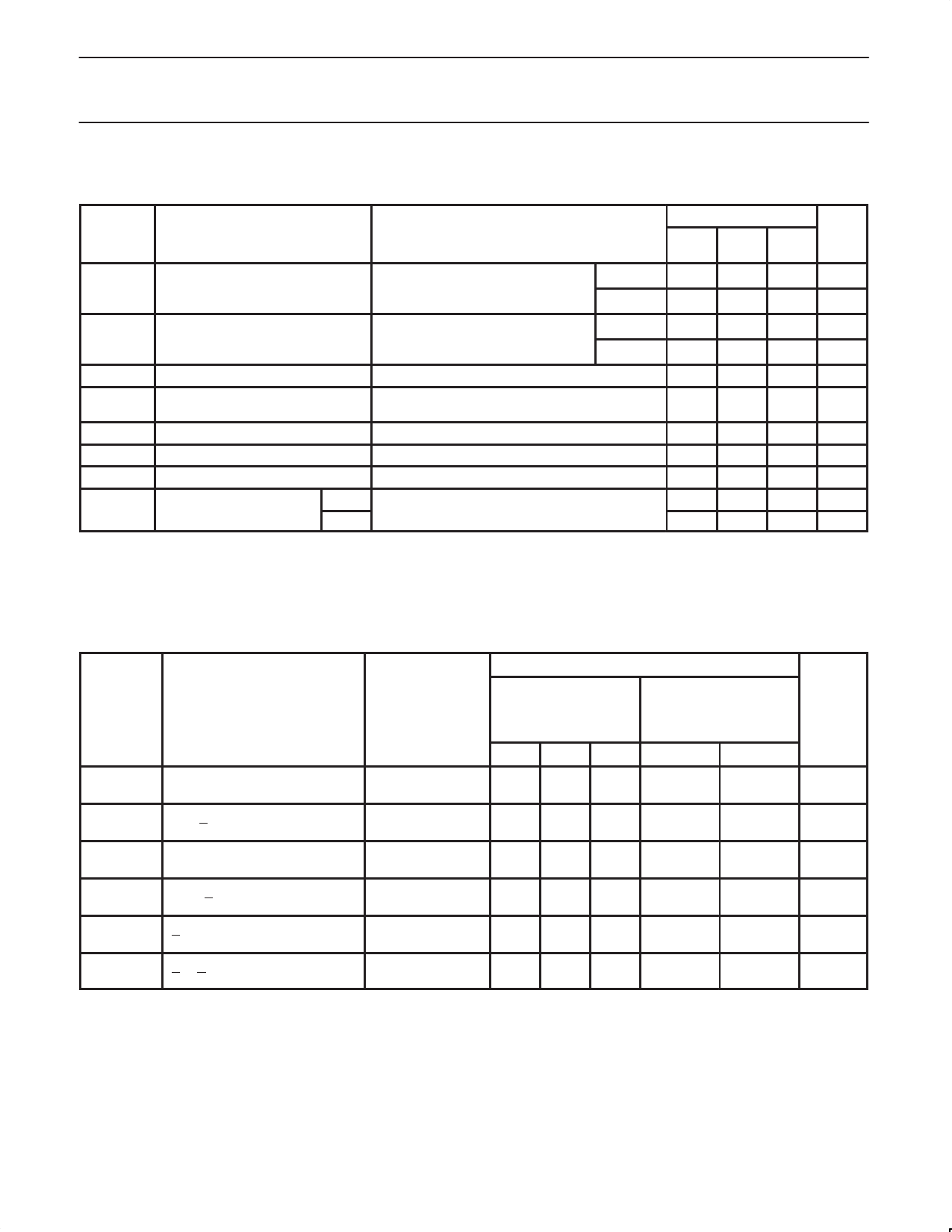
DC ELECTRICAL CHARACTERISTICS
(Over recommended operating free-air temperature range unless otherwise noted.)
SYMBOL
PARAMETER\
TEST CONDITIONSNO TAG
LIMITS
MIN
TYP
NO TAG
MAX
UNIT
VOH
High-level output voltage
VCC = MIN, VIL = MAX,
VIH = MIN, IOH = MAX
±10%VCC 2.5
V
±5%VCC 2.7
3.4
V
VOL
Low-level output voltage
VCC = MIN, VIL = MAX,
VIH = MIN, IOL = MAX
±10%VCC
±5%VCC
0.30 0.50
V
0.30 0.50
V
VIK
Input clamp voltage
VCC = MIN, II = IIK
–0.73 –1.2
V
II
Input current at maximum input
voltage
VCC = MAX, VI = 7.0V
100
µA
IIH
High-level input current
VCC = MAX, VI = 2.7V
20
µA
IIL
Low-level input current
VCC = MAX, VI = 0.5V
IOS
Short-circuit output currentNO TAG
VCC = MAX
–0.6 mA
–60
–150 mA
ICCH
ICC
Supply current (total)
ICCL
VCC = MAX
18
25
mA
17
25
mA
NOTES:
1. For conditions shown as MIN or MAX, use the appropriate value specified under recommended operating conditions for the applicable type.
2. All typical values are at VCC = 5V, Tamb = 25°C.
3. Not more than one output should be shorted at a time. For testing IOS, the use of high-speed test apparatus and/or sample-and-hold
techniques are preferable in order to minimize internal heating and more accurately reflect operational values. Otherwise, prolonged shorting
of a High output may raise the chip temperature well above normal and thereby cause invalid readings in other parameter tests. In any
sequence of parameter tests, IOS tests should be performed last.
AC ELECTRICAL CHARACTERISTICS
LIMITS
SYMBOL
PARAMETER
TEST
CONDITION
VCC = +5.0V
Tamb = +25°C
CL = 50pF
RL = 500Ω
MIN TYP MAX
VCC = +5.0V ± 10%
Tamb = 0°C to +70°C
CL = 50pF
RL = 500Ω
MIN
MAX
UNIT
tPLH
Propagation delay
tPHL
In to Y
tPLH
Propagation delay
tPHL
In to Y
tPLH
Propagation delay
tPHL
Sn to Y
tPLH
Propagation delay
tPHL
Sn to Y
tPLH
Propagation delay
tPHL
E to Y
tPLH
Propagation delay
tPHL
E to Y
Waveform NO TAG
2.5
2.5
4.5
4.5
7.0
7.0
2.5
2.5
Waveform NO TAG
2.0
1.0
4.0
2.0
7.0
4.5
2.0
1.0
Waveform 1, 2
4.5
6.5 10.0
4.0
6.0
8.5
4.0
3.5
Waveform NO TAG, 3.5
5.5
8.5
3.0
NO TAG
2.5
4.5
7.0
2.0
Waveform 1
4.0
6.5
9.0
3.0
5.0
7.0
3.5
3.0
Waveform NO TAG
2.5
2.0
4.5
3.5
6.5
5.5
2.5
1.5
7.5
7.5
ns
7.5
5.0
ns
11.0
9.5
ns
9.5
7.5
ns
9.5
7.5
ns
7.0
6.0
ns
AC WAVEFORMS
For all waveforms, VM = 1.5V
1995 Jul 17
5
Share Link: 