74VCX1632245TBR(2005) 查看數據表(PDF) - STMicroelectronics
零件编号
产品描述 (功能)
生产厂家
74VCX1632245TBR
(Rev.:2005)
(Rev.:2005)
STMicroelectronics

74VCX1632245TBR Datasheet PDF : 18 Pages
| |||
74VCX1632245
16-BIT DUAL SUPPLY BUS TRANSCEIVER
LEVEL TRANSLATOR WITH A SIDE SERIES RESISTOR
I HIGH SPEED: tPD = 4.4ns (MAX.) at TA=85°C
VCCA = 3.0V VCCB = 2.3V
I LOW POWER DISSIPATION:
ICCA = ICCB = 20µA(MAX.) at TA=85°C
I SYMMETRICAL OUTPUT IMPEDANCE:
) |IOHA| = IOLA = 8mA MIN at
t(s VCCA = 3.0V VCCB = 1.65V or 2.3V
|IOHA| = IOLA = 18mA MIN at
c VCCA = 2.3V VCCB = 1.65V)
u I BALANCED PROPAGATION DELAYS:
d tPLH ≅ tPHL
ro I POWER DOWN PROTECTION ON INPUTS
P AND OUTPUTS
I 26Ω SERIES RESISTOR ON A SIDE OUTPUTS
te I OPERATING VOLTAGE RANGE:
le VCCA(OPR) = 2.3V to 3.6V (1.2V Data
o Retention)
s VCCB(OPR) = 1.65V to 2.7V (1.2V Data
b Retention)
O I MAX DATA RATES:
- 380 Mbps (1.8V to 3.3V translation)
) 260 Mbps (<1.8V to 3.3V translation)
t(s 260 Mbps (Translate to 2.5V)
c 210 Mbps (Translate to 1.5V)
u 100 Mbps (Translate to 1.2V)
d I PIN AND FUNCTION COMPATIBLE WITH
ro 74 SERIES 16245
P I LATCH-UP PERFORMANCE EXCEEDS
te 500mA (JESD 17)
I ESD PERFORMANCE:
le HBM > 2000V (MIL STD 883 method 3015);
o MM > 200V
Obs DESCRIPTION
TSSOP
TFBGA
µTFBGA
Table 1: Order Codes
PACKAGE
TSSOP48
TFBGA54
µTFBGA42
T&R
74VCX1632245TTR
74VCX1632245LBR
74VCX1632245TBR
isolated. The A-port interfaces with the 3V bus, the
B-port with the 2.5V and 1.8V bus.
All inputs are equipped with protection circuits
against static discharge, giving them 2KV ESD im-
munity and transient excess voltage. All floating
bus terminals during High Z State must be held
HIGH or LOW.
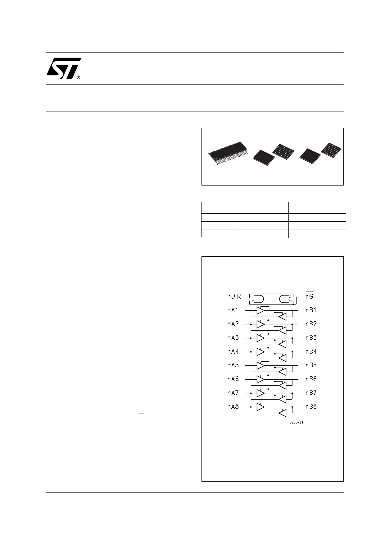
Figure 1: Logic Diagram
The 74VCX1632245 is a dual supply low voltage
CMOS 16-BIT BUS TRANSCEIVER fabricated
with sub-micron silicon gate and five-layer metal
wiring C2MOS technology. Designed for use as an
interface between a 3.3V bus and a 2.5V or 1.8V
bus in a mixed 3.3V/1.8V,3.3V/2.5V and 2.5V/
1.8V supply systems, it achieves high speed
operation while maintaining the CMOS low power
dissipation.
This IC is intended for two-way asynchronous
communication between data buses and the
direction of data transmission is determined by
nDIR inputs. The enable inputs nG can be used to
disable the device so that the buses are effectively
n = 1, 2
March 2005
Rev. 14
1/18
Share Link: