ADC0808S125HW 查看數據表(PDF) - NXP Semiconductors.
零件编号
产品描述 (功能)
生产厂家
ADC0808S125HW Datasheet PDF : 23 Pages
| |||
NXP Semiconductors
ADC0808S125/250
Single 8-bit ADC, up to 125 MHz or 250 MHz
Table 3. Pin type description
Type
Description
I
input
O
output
I(CMOS)
1.8 V CMOS level input
O(CMOS)
1.8 V CMOS level output
P
power supply
G
ground
7. Functional description
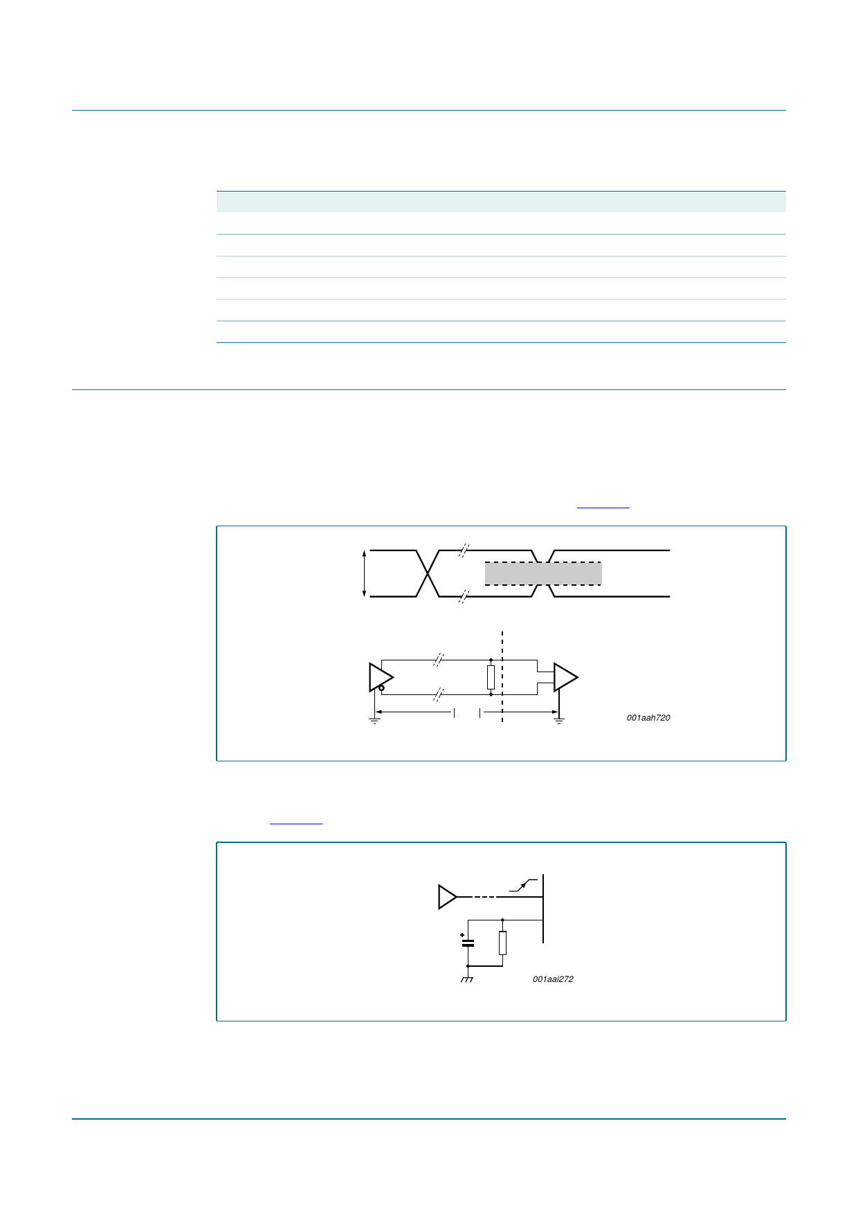
7.1 CMOS/LVDS clock input
The circuit has two clock inputs CLK+ and CLK−, with two modes of operation:
• LVDS mode: CLK+ and CLK− inputs are at differential LVDS levels. An external
resistor of between 80 Ω and 120 Ω is required; see Figure 3.
VO(dif)
undefined state
maximum Vidth
minimum Vidth
LVDS
DRIVER
RECEIVER
CLK+
Vgpd
CLK−
001aah720
Fig 3. LVDS clock input
• 1.8 V CMOS mode: CLK+ input is at 1.8 V CMOS level and sampling is done on the
rising edge of the clock input signal. In this case pin CLK− must be grounded;
see Figure 4.
CMOS
DRIVER
CLK+
CLK−
Fig 4. CMOS clock input
001aai272
ADC0808S125_ADC0808S250_3
Product data sheet
Rev. 03 — 24 February 2009
© NXP B.V. 2009. All rights reserved.
5 of 23
Share Link: 