CS5203A-1 查看數據表(PDF) - ON Semiconductor
零件编号
产品描述 (功能)
生产厂家
CS5203A-1 Datasheet PDF : 10 Pages
| |||
CS5203A−1, CS5203A−2, CS5203A−3, CS5203A−5
ORDERING INFORMATION
Device
Type
Package
Shipping†
CS5203A−1GT3
CS5203A−1GDP3
CS5203A−1GDPR3
3.0 A, Adj. Output
3.0 A, Adj. Output
3.0 A, Adj. Output
TO−220−3, STRAIGHT
D2PAK−3
D2PAK−3
50 Units / Rail
50 Units / Rail
750 / Tape & Reel
CS5203A−2GT3
CS5203A−2GDP3
CS5203A−2GDPR3
CS5203A−2GDPR3G
CS5203A−2GDPSR3
3.0 A, 1.5 V Output
3.0 A, 1.5 V Output
3.0 A, 1.5 V Output
3.0 A, 1.5 V Output
3.0 A, 1.5 V Output
TO−220−3, STRAIGHT
D2PAK−3
D2PAK−3
D2PAK−3
(Pb−Free)
D2PAK−3
50 Units / Rail
50 Units / Rail
750 / Tape & Reel
750 / Tape & Reel
750 / Tape & Reel
CS5203A−3GT3
CS5203A−3GDP3
CS5203A−3GDPR3
CS5203A−3GDPSR3
3.0 A, 3.3 V Output
3.0 A, 3.3 V Output
3.0 A, 3.3 V Output
3.0 A, 3.3 V Output
TO−220−3, STRAIGHT
D2PAK−3
D2PAK−3
D2PAK−3
50 Units / Rail
50 Units / Rail
750 / Tape & Reel
750 / Tape & Reel
CS5203A−5GT3
3.0 A, 5.0 V Output
TO−220−3, STRAIGHT
50 Units / Rail
†For information on tape and reel specifications, including part orientation and tape sizes, please refer to our Tape and Reel Packaging
Specifications Brochure, BRD8011/D.
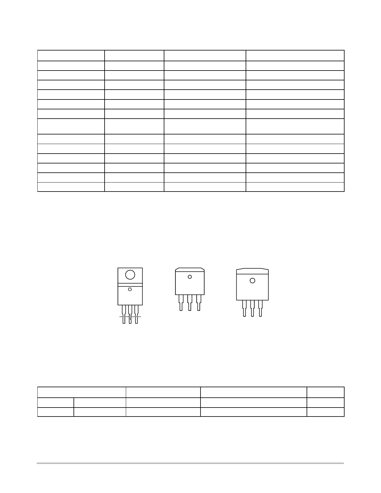
TO−220−3
T SUFFIX
CASE 221A
MARKING DIAGRAMS
D2PAK−3
DP SUFFIX
CASE 418AB
D2PAK−3
DPS SUFFIX
CASE 418F
CS
5203A−x
AWLYWW
1
CS
5203A−x
AWLYWW
1
x
= 1, 2, 3, or 5
A
= Assembly Location
WL, L = Wafer Lot
YY, Y = Year
WW, W = Work Week
CS
5203A−x
AWLYYWW
1
PACKAGE THERMAL DATA
Parameter
TO−220−3
RqJC
Typical
1.6
RqJA
Typical
50
*Depending on thermal properties of substrate. RqJA = RqJC + RqCA.
D2PAK−3
1.6
10−50*
Unit
°C/W
°C/W
http://onsemi.com
8
Share Link: 