IDT72413L25P(2003) 查看數據表(PDF) - Integrated Device Technology
零件编号
产品描述 (功能)
生产厂家
IDT72413L25P Datasheet PDF : 10 Pages
| |||
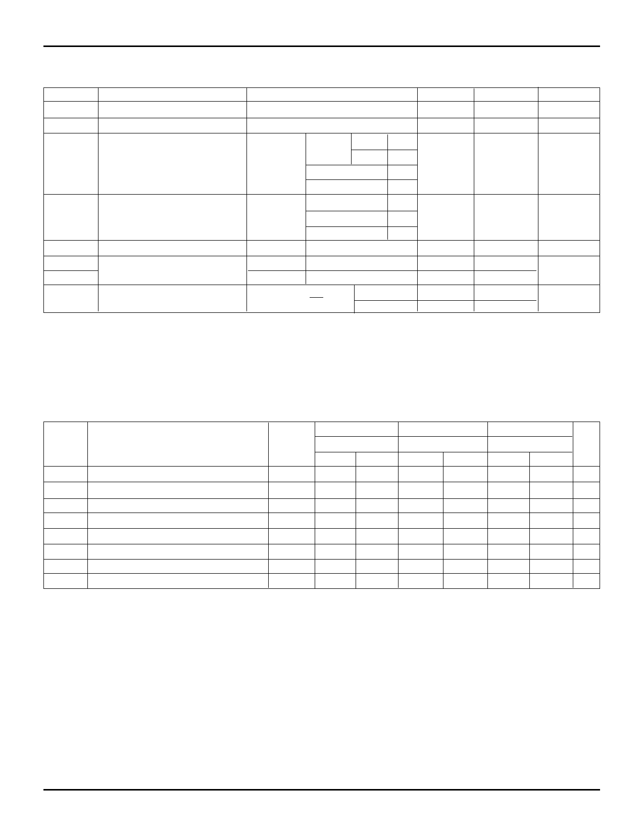
IDT72413 CMOS PARALLEL FIFO WITH FLAGS
64 x 5
COMMERCIAL TEMPERATURE RANGE
OPERATING CONDITIONS
(Commercial: VCC = 5.0V ± 10%, TA = 0°C to +70°C)
Symbol
tSIH(1)
tSIL(1)
tIDS
tIDH
tSOH(1)
tSOL
tMRW
tMRS
Parameter
Shift in HIGH Time
Shift in LOW TIme
Input Data Set-up
Input Data Hold Time
Shift Out HIGH Time
Shift Out LOW Time
Master Reset Pulse
Master Reset Pulse to SI
Figure
2
2
2
2
5
5
8
8
IDT72413L45
Min.
Max.
9
—
11
—
0
—
13
—
9
—
11
—
20
—
20
—
Commercial
IDT72413L35
Min.
Max.
9
—
17
—
0
—
15
—
9
—
17
—
30
—
35
—
IDT72413L25
Min.
Max. Unit
16
—
ns
20
—
ns
0
—
ns
25
—
ns
16
—
ns
20
—
ns
35
—
ns
35
—
ns
NOTE:
1. Since the FIFO is a very high-speed device, care must be excercised in the design of the hardware and timing utilized within the design. Device grounding and decoupling
are crucial to correct operation as the FIFO will respond to very small glitches due to long reflective lines, high capacitances and/or poor supply decoupling and grounding.
A monolithic ceramic capacitor of 0.1µF directly between VCC and GND with very short lead length is recommended.
AC ELECTRICAL CHARACTERISTICS
(Commercial: VCC = 5.0V ± 10%, TA = 0°C to +70°C)
Commercial
Symbol
fIN
tIRL(1)
tIRH(1)
fOUT
tORL(1)
tORH(1)
tODH(1)
tODS
tPT
tMRORL
tMRIRH(3)
tMRIRL(2)
tMRQ
tMRHF
tMRAFE
tIPH(3)
tOPH(3)
tORD(3)
tAEH
tAEL
tAFL
tAFH
tHFH
tHFL
tPHZ(3)
tPLZ(3)
tPLZ(3)
tPHZ(3)
Shift In Rate
Parameter
Shift In ↑ to Input Ready LOW
Shift In ↓ to Input Ready HIGH
Shift Out Rate
Shift Out ↓ to Output Ready LOW
Shift Out ↓ to Output Ready HIGH
Output Data Hold Previous Word
Output Data Shift Next Word
Data Throughput or "Fall-Through"
Master Reset ↓ to Output Ready LOW
Master Reset ↑ to Input Ready HIGH
Master Reset ↓ to Input Ready LOW
Master Reset ↓ to Outputs LOW
Master Reset ↓ to Half-Full Flag
Master Reset ↓ to AF/E Flag
Input Ready Pulse HIGH
Output Ready Pulse HIGH
Output Ready ↑ HIGH to Valid Data
Shift Out ↑ to AF/E HIGH
Shift In ↑ to AF/E
Shift Out ↑ to AF/E LOW
Shift In ↑ to AF/E HIGH
Shift In ↑ to HF HIGH
Shift Out ↑ to HF LOW
Output Disable Delay
Output Enable Delay
Figure
2
2
2
5
5
5
5
5
4, 7
8
8
8
8
8
8
4
7
5
9
9
10
10
11
11
12
12
12
12
IDT72413L45
Min.
Max.
—
45
—
18
—
18
—
45
—
18
—
19
5
—
—
19
—
25
—
25
—
25
—
25
—
20
—
25
—
25
5
—
5
—
—
5
—
28
—
28
—
28
—
28
—
28
—
28
—
12
—
12
—
15
—
15
IDT72413L35
Min.
Max.
—
35
—
18
—
20
—
35
—
18
—
20
5
—
—
20
—
28
—
28
—
28
—
28
—
25
—
28
—
28
5
—
5
—
—
5
—
28
—
28
—
28
—
28
—
28
—
28
—
12
—
12
—
15
—
15
IDT72413L25
Min.
Max. Unit
—
25 M H z
—
28
ns
—
25
ns
—
25 M H z
—
28
ns
—
25
ns
5
—
ns
—
20
ns
—
40
ns
—
30
ns
—
30
ns
—
30
ns
—
35
ns
—
40
ns
—
40
ns
5
—
ns
5
—
ns
—
7
ns
—
40
ns
—
40
ns
—
40
ns
—
40
ns
—
40
ns
—
40
ns
—
15
ns
—
15
—
20
ns
—
20
NOTES:
1. Since the FIFO is a very high-speed device, care must be taken in the design of the hardware and the timing utilized within the design. Device grounding and decoupling
are crucial to correct operation as the FIFO will respond to very small glitches due to long reflective lines, high capacitances and/or poor supply decoupling and grounding.
A monolithic ceramic capacitor of 0.1µF directly between VCC and GND with very short lead length is recommended.
2. If the FIFO is full, (IR = HIGH), MR ↑ forces IR to go LOW, and MR ↓ causes IR to go HIGH.
3. Guaranteed by design but not currently tested.
3
Share Link: 