MAX6972 查看數據表(PDF) - Maxim Integrated
零件编号
产品描述 (功能)
生产厂家
MAX6972 Datasheet PDF : 23 Pages
| |||
16-Output PWM LED Drivers
for Message Boards
Power-Supply Considerations
The MAX6972/MAX6973 operate with a power-supply
voltage of 3.0V to 3.6V. Bypass the VDD power supply
to GND with a 0.1µF ceramic capacitor as close as
possible to the device pins. If the LED supply is shared
with the VDD supply, adequately decouple the VDD
supply with bulk capacitance to ensure that the fast-
rising, high-current LED drive currents do not cause
transient dips in VDD.
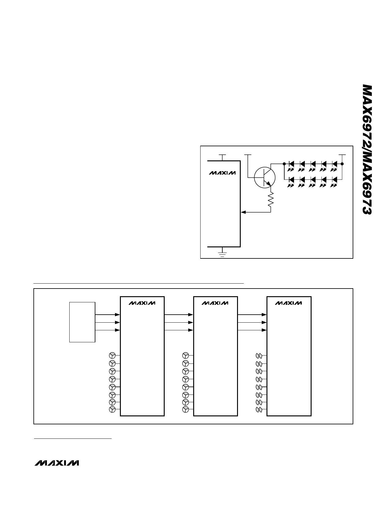
Driving LEDs from a Supply Higher than 7V
An external npn transistor in a cascode configuration
extends the output drive voltage above 7V. The external
pass transistor’s emitter clamps to a VBE below its
base, which is connected to the MAX6972/MAX6973’s
supply voltage. An optional emitter resistor reduces the
voltage drop across the MAX6972/MAX6973’s output
transistor and effectively takes the dissipation off the
device into the resistor. The external transistor’s collector
current is equal to its emitter current (less a small base
current), and the MAX6972/MAX6973 accurately
control the emitter current with a constant current sink
driver structure.
Example of using an external npn transistor:
VDD = 3.3V ±5%, IOUT = 55mA, external pass transistor
VBE = 0.7V - 1V at 55mA emitter current.
For best output current accuracy, design VO to be at
least 1.2V:
R1(MAX) = (3.15 - 1 - 1.2) / 0.055 = 17.3Ω, so choose
R1 = 15Ω
hence,
VO(MIN) = 3.15 - 1 - (15 x 0.055) = 1.325V and VO(MAX)
= 3.45 - 0.7 - (15 x 0.055) = 1.925V.
+3.3V
+3.3V
+24V
VDD
MAX6972
Q1
MAX6973
R1
Y0
Y1
Y2
Y3
Y4
Y5
Y6
GND Y7
55mA
Figure 13. External Cascode npn Transistor
Typical Operating Circuit
SYSTEM
CLK
DATA
LOAD
MAX6972
CLKI
CLKO
DINI
DINO
LOADI
LOADO
16 RG LEDs
Y0/Z0
Y1/Z1
Y2/Z2
Y3/Z3
Y4/Z4
Y5/B5
Y6/Z6
Y7/Z7
MAX6972
CLKI
CLKO
DINI
DINO
LOADI
LOADO
MAX6972
CLKI
CLKO
DINI
DINO
LOADI
LOADO
Y0/Z0
Y1/Z1
Y2/Z2
Y3/Z3
Y4/Z4
Y5/B5
Y6/Z6
Y7/Z7
16 BLUE LEDs
Y0/Z0
Y1/Z1
Y2/Z2
Y3/Z3
Y4/Z4
Y5/B5
Y6/Z6
Y7/Z7
PROCESS: BiCMOS
Chip Information
______________________________________________________________________________________ 21
Share Link: 