NX25F011B 查看數據表(PDF) - Unspecified
零件编号
产品描述 (功能)
生产厂家
NX25F011B Datasheet PDF : 37 Pages
| |||
NX25F011B
NX25F021B
NX25F041B
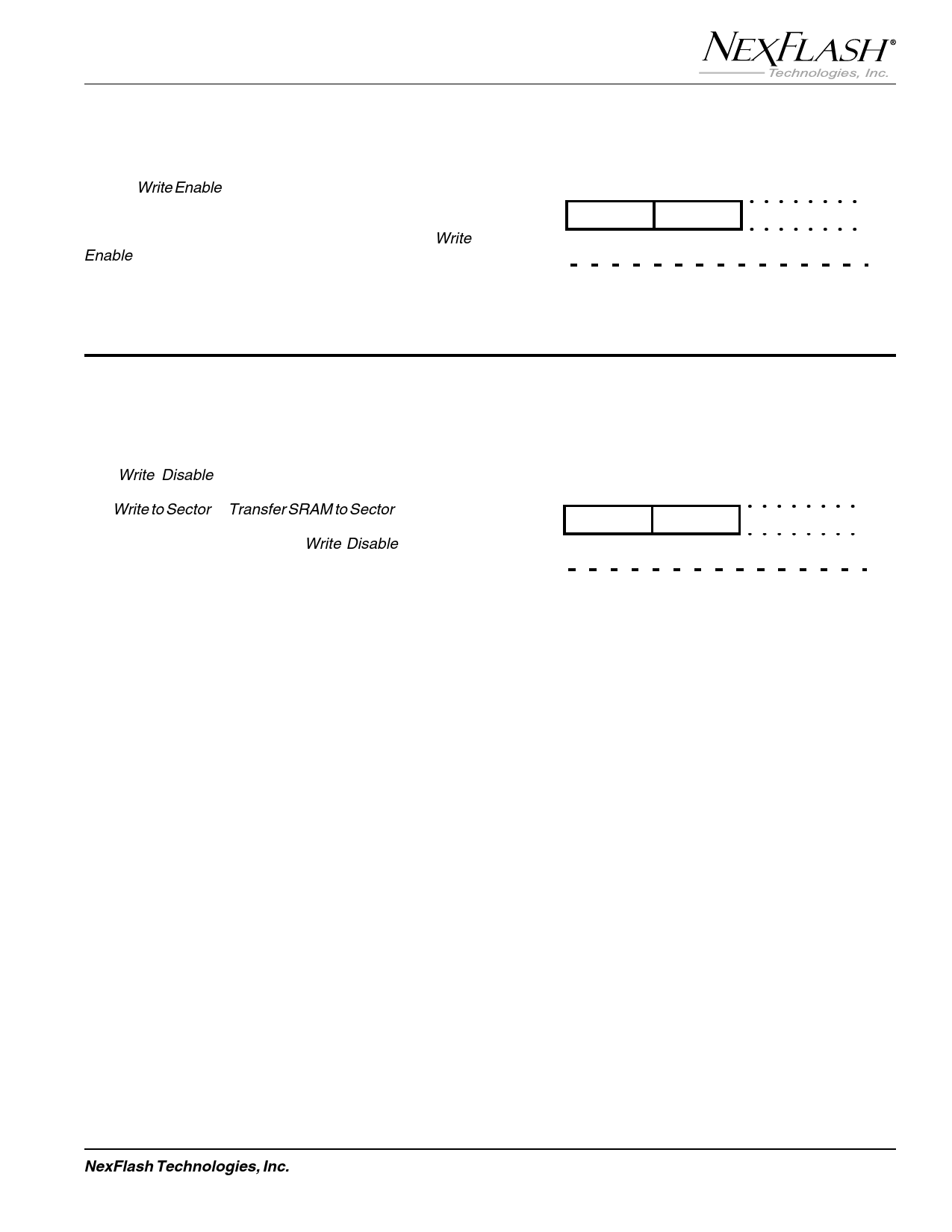
Write Enable (06H)
Upon power-up, the Flash memory array is write- protected
until the Write Enable command (06H) has been issued. The
WP pin must be inactive while writing the command for the
write enable to be accepted. The status of the device’s write
protect state can be read in the status register. The Write
Enable command sequence is completed by asserting CS
high after eight additional clocks.
Write Enable
Command 8 Clocks
SI
06H
00H
SO
Write Disable (04H)
The Write Disable command (04H) protects the Flash
memory array from being programmed. Once issued, fur-
ther Write to Sector or Transfer SRAM to Sector commands
will be ignored. The status of the write protect state can be
read in the status register. The Write Disable command
sequence is completed by asserting CS high after eight
additional clocks.
Write Disable
Command 8 Clocks
SI
04H
00H
SO
NexFlash Technologies, Inc.
PRELIMINARY NXSF016F-1201
12/12/01 ©
1
2
3
4
5
6
7
8
9
10
11
12
17
Share Link: 