OR2C04A وں¥çœ‹و•¸و“ڑè،¨ï¼ˆPDF) - Lattice Semiconductor
零ن»¶ç¼–هڈ·
ن؛§ه“پوڈڈè؟° (هٹں能)
ç”ںن؛§هژ‚ه®¶
OR2C04A Datasheet PDF : 192 Pages
| |||
ORCA Series 2 FPGAs
Data Sheet
January 2002
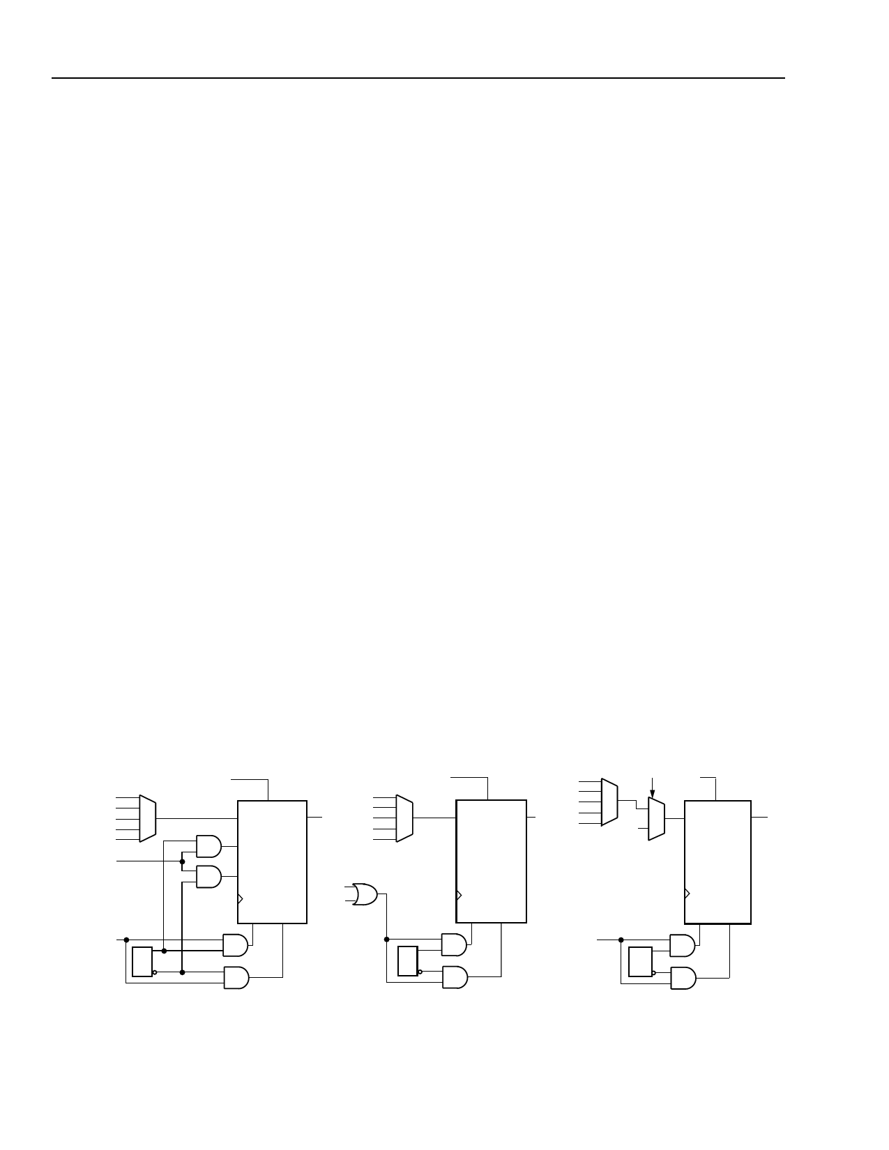
Programmable Logic Cells (continued)
The set/reset operation of the latch/FF is controlled by
two parameters: reset mode and set/reset value. When
the global set/reset (GSRN) or local set/reset (LSR) are
inactive, the storage element operates normally as a
latch or FF. The reset mode is used to select a synchro-
nous or asynchronous LSR operation. If synchronous,
LSR is enabled only if clock enable (CE) is active. For
the Series 2 series, a new option called the LSR prior-
ity allows the synchronous LSR to have priority over the
CE input, thereby setting or resetting the FF indepen-
dent of the state of CE. The clock enable is supported
on FFs, not latches. The clock enable function is imple-
mented by using a two-input multiplexer on the FF
input, with one input being the previous state of the FF
and the other input being the new data applied to the
FF. The select of this two-input multiplexer is clock
enable (CE), which selects either the new data or the
previous state. When CE is inactive, the FF output does
not change when the clock edge arrives.
The GSRN signal is only asynchronous, and it sets/
resets all latches/FFs in the FPGA based upon the set/
reset conï¬پguration bit for each latch/FF. The set/reset
value determines whether GSRN and LSR are set or
reset inputs. The set/reset value is independent for
each latch/FF.
If the local set/reset is not needed, the latch/FF can be
conï¬پgured to have a data front-end select. Two data
inputs are possible in the front-end select mode, with
the LSR signal used to select which data input is used.
The data input into each latch/FF is from the output of
its associated QLUT F[3:0] or direct from WD[3:0],
bypassing the LUT. In the front-end data select mode,
both signals are available to the latches/FFs.
For PLCs that are in the two outside rows or columns of
the array, the latch/FFs can have two inputs in addition
to the F and WD inputs mentioned above. One input is
from an I/O pad located at the PIC closest to either the
left or right of the given PLC (if the PLC is in the left two
columns or right two columns of the array). The other
input is from an I/O pad located at the closest PIC
either above or below the given PLC (if the PLC is in
the top or the bottom two rows). It should be noted that
both inputs are available for a 2 x 2 array of PLCs in
each corner of the array. For the entire array of PLCs, if
either or both of these inputs is unavailable, the latch/
FF data input can be tied to a logic 0 instead (the
default).
To speed up the interface between signals external to
the FPGA and the latches/FFs, there are direct paths
from latch/FF outputs to the I/O pads. This is done for
each PLC that is adjacent to a PIC.
The latches/FFs can be conï¬پgured in three modes:
1. Local synchronous set/reset: the input into the PFU’s
LSR port is used to synchronously set or reset each
latch/FF.
2. Local asynchronous set/reset: the input into LSR
asynchronously sets or resets each latch/FF.
3. Latch/FF with front-end select: the data select signal
(actually LSR) selects the input into the latches/FFs
between the LUT output and direct data in.
For all three modes, each latch/FF can be indepen-
dently programmed as either set or reset. Each latch/
FF in the PFU is independently conï¬پgured to operate
as either a latch or flip-flop. Figure 18 provides the logic
functionality of the front-end select, global set/reset,
and local set/reset operations.
PDINTB
PDINLR
F
WD
LOGIC 0
LSR
GSRN
CD
CE
CE
D
Q
S_SET
PDINTB
PDINLR
F
WD
LOGIC 0
S_RESET
CLK
GSRN
LSR
SET RESET
CE
PDINTB
PDINLR
D
CE
Q
F
WD
LOGIC 0
LSR CE
CE
D
Q
WD
CLK
SET RESET
CLK
SET RESET
GSRN
CD
CD
Note: CD = conï¬پguration data.
Figure 18. Latch/FF Set/Reset Conï¬پgurations
5-2839(F).a
16
Lattice Semiconductor
Share Link: 