HYB39S16400AT-10 查看數據表(PDF) - Siemens AG
零件编号
产品描述 (功能)
生产厂家
HYB39S16400AT-10 Datasheet PDF : 22 Pages
| |||
HYB 39S16400/800/160AT-8/-10
16 MBit Synchronous DRAM
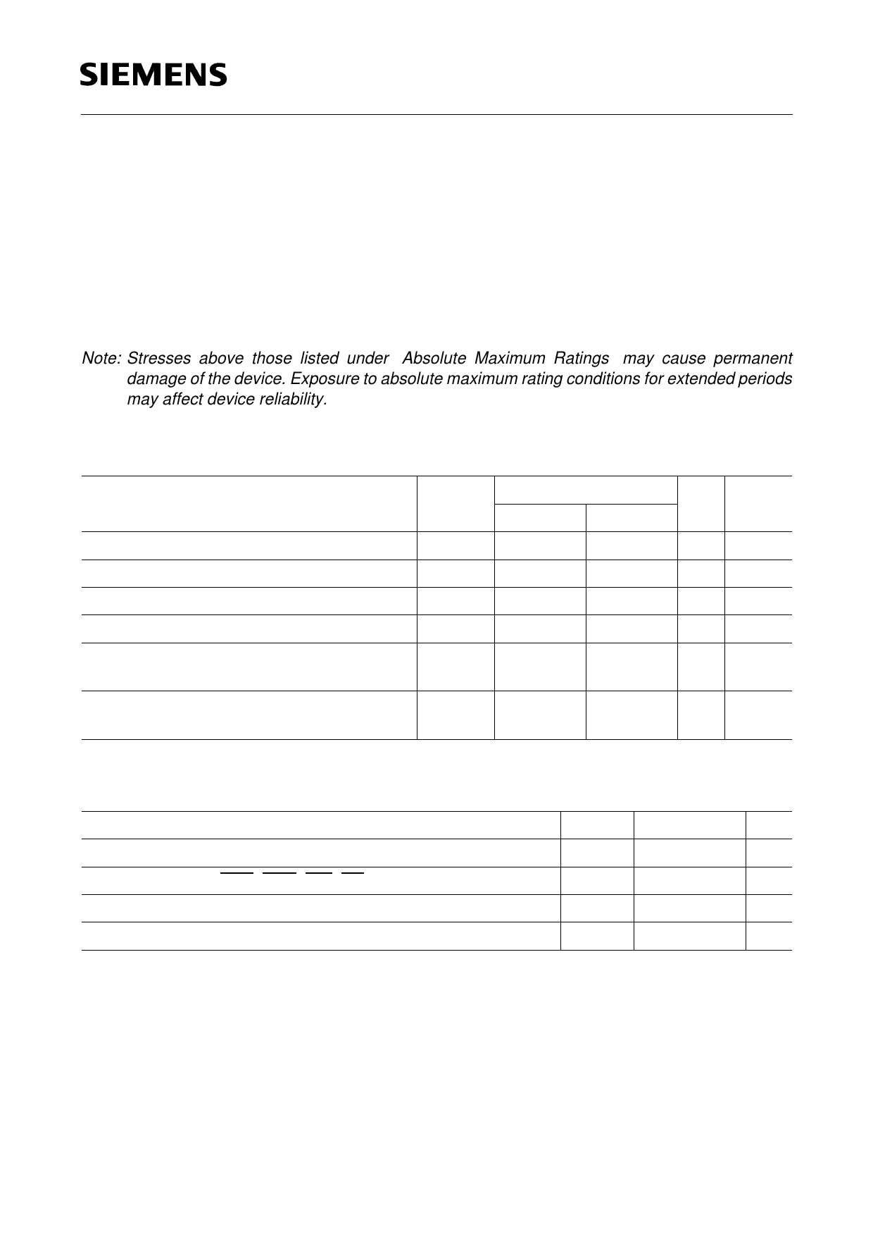
Absolute Maximum Ratings
Operating temperature range ........................................................................................ 0 to + 70 °C
Storage temperature range..................................................................................... – 55 to + 150 °C
Input/output voltage .......................................................................... – 0.5 to min (VCC + 0.5, 4.6) V
Power supply voltage VDD / VDDQ ............................................................................. – 1.0 to + 4.6 V
Power Dissipation ....................................................................................................................... 1 W
Data out current (short circuit) ................................................................................................ 50 mA
Note: Stresses above those listed under “Absolute Maximum Ratings” may cause permanent
damage of the device. Exposure to absolute maximum rating conditions for extended periods
may affect device reliability.
Recommended Operation and Characteristics for LV-TTL Versions
TA = 0 to 70 °C; VSS = 0 V; VDD, VDDQ = 3.3 V ± 0.3 V
Parameter
Symbol
Limit Values
min.
max.
Input high voltage
Input low voltage
Output high voltage (IOUT = – 2.0 mA)
Output low voltage (IOUT = 2.0 mA)
Input leakage current, any input
(0 V < VIN < VDDQ, all other inputs = 0 V)
Output leakage current
(DQ is disabled, 0 V < VOUT < VCC)
VIH
2.0
VIL
– 0.3
VOH
2.4
VOL
–
II(L)
– 10
IO(L)
– 10
VCC + 0.3
0.8
–
0.4
10
10
Unit Notes
V
1, 2
V
1, 2
V
V
µA
µA
Capacitance
TA = 0 to 70 °C; VDD = 3.3 V ± 0.3 V, f = 1 MHz
Parameter
Input capacitance (A0 to A11)
Input capacitance (RAS, CAS, WE, CS, CLK, CKE, DQM)
Output capacitance (DQ)
VREF
Symbol max. Values Unit
CI1
4
pF
CI2
4
pF
CIO
5
pF
CREF
8
pF
Semiconductor Group
14
1998-10-01
Share Link: 