MAX8795AGCJ(2007) 查看數據表(PDF) - Maxim Integrated
零件编号
产品描述 (功能)
生产厂家
MAX8795AGCJ Datasheet PDF : 30 Pages
| |||
TFT-LCD DC-DC Converter with
Operational Amplifiers
Table 2. Component Suppliers
SUPPLIER
PHONE
Fairchild
Sumida
TDK
Toshiba
408-822-2000
847-545-6700
847-803-6100
949-455-2000
FAX
408-822-2102
847-545-6720
847-390-4405
949-859-3963
WEBSITE
www.fairchildsemi.com
www.sumida.com
www.component.tdk.com
www.toshiba.com/taec
VCN
VIN
IN
STEP-UP
CONTROLLER
LX
FB
COMP
PGND
AGND
MAX8795A
GATE-ON
CONTROLLER
DRVP
FBP
SRC
COM
SWITCH
CONTROL
DRN
SUP
NEG1
OUT1 OP1
POS1
NEG2
GATE-OFF
CONTROLLER
REF
DEL
CTL
DRVN
FBN
REF
NEG4
OUT2 OP2
POS2
OP4 OUT4
POS4
NEG5
OUT3
OP3
POS3
OUT5
OP5
EP
BGND
POS5
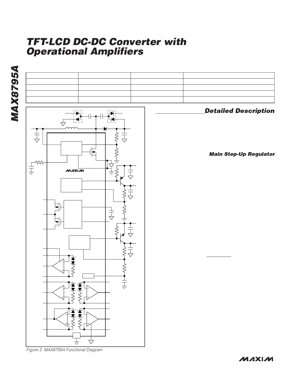
Figure 2. MAX8795A Functional Diagram
VCP
VMAIN
VCP
VGON
VCN
VGOFF
Detailed Description
The MAX8795A contains a high-performance step-up
switching regulator, two low-cost linear-regulator con-
trollers, multiple high-current operational amplifiers,
and startup timing and level-shifting functionality useful
for active-matrix TFT LCDs. Figure 2 shows the
MAX8795A functional diagram.
Main Step-Up Regulator
The main step-up regulator employs a current-mode,
fixed-frequency PWM architecture to maximize loop
bandwidth and provide fast transient response to
pulsed loads typical of TFT-LCD panel source drivers.
The 1.2MHz switching frequency allows the use of low-
profile inductors and ceramic capacitors to minimize
the thickness of LCD panel designs. The integrated
high-efficiency MOSFET and the IC’s built-in digital
soft-start functions reduce the number of external com-
ponents required while controlling inrush currents. The
output voltage can be set from VIN to 18V with an exter-
nal resistive voltage-divider.
The regulator controls the output voltage and the power
delivered to the output by modulating the duty cycle (D)
of the internal power MOSFET in each switching cycle.
The duty cycle of the MOSFET is approximated by:
D ≈ VMAIN − VIN
VMAIN
Figure 3 shows the functional diagram of the step-up
regulator. An error amplifier compares the signal at FB
to 1.233V and changes the COMP output. The voltage
at COMP sets the peak inductor current. As the load
varies, the error amplifier sources or sinks current to the
COMP output accordingly to produce the inductor peak
current necessary to service the load. To maintain sta-
bility at high duty cycles, a slope-compensation signal
is summed with the current-sense signal.
On the rising edge of the internal clock, the controller sets
a flip-flop, turning on the n-channel MOSFET and applying
the input voltage across the inductor. The current through
the inductor ramps up linearly, storing energy in its
magnetic field. Once the sum of the current-feedback
signal and the slope compensation exceeds the COMP
16 ______________________________________________________________________________________
Share Link: 