AD8231-EVALZ 查看數據表(PDF) - Analog Devices
零件编号
产品描述 (功能)
生产厂家
AD8231-EVALZ Datasheet PDF : 24 Pages
| |||
AD8231
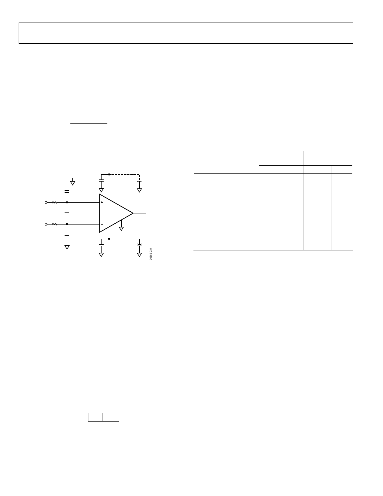
RF INTERFERENCE
RF rectification is often a problem when amplifiers are used in
applications where there are strong RF signals. The disturbance
can appear as a small dc offset voltage. High frequency signals
can be filtered with a low-pass, RC network placed at the
input of the instrumentation amplifier, as shown in Figure 52.
The filter limits the input signal bandwidth according to the
following relationship
FilterFreqDiff =
1
2π R(2CD + CC)
FilterFreqCM = 1
2π RCC
where CD ≥ 10CC.
+VS
R
4.02kΩ
R
4.02kΩ
CC
1nF
CD
10nF
CC
1nF
0.1µF
10µF
+INA
AD8231
VOUT
REF
–INA
0.1µF
10µF
–VS
Figure 52. RFI Suppression
Figure 52 shows an example where the differential filter frequency
is approximately 2 kHz, and the common-mode filter frequency
is approximately 40 kHz.
Values of R and CC should be chosen to minimize RFI. Mismatch
between the R × CC at the positive input and the R × CC at the
negative input degrades the CMRR of the AD8231. By using a
value of CD that is ten times larger than the value of CC, the
effect of the mismatch is reduced and performance is improved.
COMMON-MODE INPUT VOLTAGE RANGE
The 3-op amp architecture of the AD8231 applies gain and then
removes the common-mode voltage. Therefore, internal nodes
in the AD8231 experience a combination of both the gained
signal and the common-mode signal. This combined signal can
be limited by the voltage supplies even when the individual input
and output signals are not. To determine whether the signal could
be limited, refer to Figure 12 through Figure 14 or use the
following formula
−VS + 0.04 V < VCM
±
VDIFF
× Gain
2
< + VS
−
0.04
V
If more common-mode range is required, the simplest solution is
to apply less gain in the instrumentation amplifier. The extra op
amp can be used to provide another gain stage after the in-amp.
Because the AD8231 has good offset and noise performance at low
gains, applying less gain in the instrumentation amplifier generally
has a limited impact on the overall system performance.
REDUCING NOISE
Because the AD8231 has no 1/f noise, reducing the bandwidth
corresponds directly to less noise. Table 8 shows the AD8231
performance at a gain of 1 at different bandwidths, assuming a
2-pole Butterworth filter roll off.
Table 8. AD8231 noise at various bandwidths
Bandwidth
(Hz)
Noise
(μV rms)
SNR
Single-Ended1
dB
Bits
SNR Differential
Output2
dB
Bits
1
0.07
148.3 24.3 154.3
25.3
3.2
0.12
143.2 23.5 149.2
24.5
10
0.21
138.3 22.7 144.3
23.7
32
0.37
133.2 21.8 139.2
22.8
100
0.66
128.3 21.0 137.63 22.0
320
1.17
123.2 20.2 129.2
21.2
1k
2.07
118.3 19.3 124.3
20.3
3.2 k
3.71
113.2 18.5 119.2
19.5
10 k
6.55
108.3 17.7 117.3
18.7
32 k
11.73
103.2 16.9 109.2
17.9
1 SNR for single-ended output configuration calculated with output signal of
4.8 V p-p, which corresponds to 1.697 V rms.
2 SNR for differential output configuration calculated with output signal of
9.6 V p-p, which corresponds to 3.397 V rms.
The AD8231 has two clocks: an auto-zero clock at 3.4 kHz and
a commutating clock at 54 kHz. While the auto-zero clock has
negligible energy and can generally be ignored, the commutating
clock has enough energy to significantly affect the noise of the
part. Therefore, in applications where low noise is critical, limiting
the bandwidth of the system below 54 kHz is recommended.
Rev. A | Page 20 of 24
Share Link: 