TDA8946 查看數據表(PDF) - Philips Electronics
零件编号
产品描述 (功能)
生产厂家
TDA8946 Datasheet PDF : 23 Pages
| |||
Philips Semiconductors
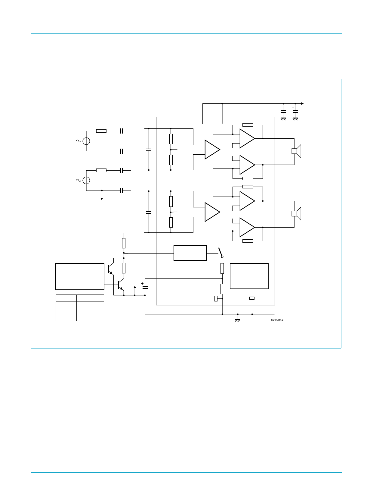
14. Application information
TDA8946J
2 x 15 W stereo BTL audio amplifier
Rs
220 nF
Symmetrical
input
Ci
220 nF
Rs
220 nF
Asymmetrical
input
Ci
signal
GND
220 nF
IN1− 8
1.5
nF
6
IN1+
IN2− 9
1.5
nF
VCC
R
12
IN2+
MODE 10
C1
MICROCONTROLLER
C2
MODE
Standby
Mute
On
C1 C2
00
01
10
R
signal
GND
SVR 11
10
µF
100 nF
3
16
30 kΩ
+VCC
1000 µF
Ri
45 kΩ
1/2 VCC
Ri
45 kΩ
−
−+
+
−
+
1/2 VCC
+
−
TDA8946J
30 kΩ
1 OUT1−
RL
8Ω
4 OUT1+
Ri
45 kΩ
1/2 VCC
Ri
45 kΩ
−
−+
+
−
+
1/2 VCC
+
−
STANDBY/
MUTE LOGIC
VCC
30 kΩ
14 OUT2−
RL
8Ω
17 OUT2+
20 kΩ
1/2 VCC
20 kΩ
SHORT CIRCUIT
AND
TEMPERATURE
PROTECTION
2
15
GND
MGU014
Fig 14. Application diagram.
14.1 Printed-circuit board (PCB)
14.1.1 Layout and grounding
For a high system performance level certain grounding techniques are essential.
The input reference grounds have to be tied with their respective source grounds and
must have separate tracks from the power ground tracks; this will prevent the large
(output) signal currents from interfering with the small AC input signals.
The small-signal ground tracks should be physically located as far as possible from
the power ground tracks. Supply and output tracks should be as wide as possible for
delivering maximum output power.
9397 750 06863
Product specification
Rev. 02 — 14 March 2000
© Philips Electronics N.V. 2000. All rights reserved.
14 of 23
Share Link: 