SA25F020LMLX 查看數據表(PDF) - Saifun Semiconductors
零件编号
产品描述 (功能)
生产厂家
SA25F020LMLX Datasheet PDF : 37 Pages
| |||
Serial Interface
Description
SPI Modes
These devices can be driven by a
microcontroller with its SPI peripheral
running in either of the two following
modes:
•= CPOL=0, CPHA=0
•= CPOL=1, CPHA=1
CPOL CPHA
0
0
CS
1
1
CS
SA25F020 Advanced Information
SAIFUN
14
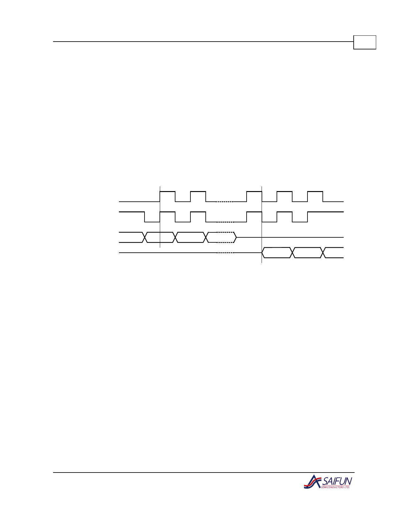
In both of these modes, input data is
latched on the rising edge of SCK, and
output data is available from the falling
edge of SCK. The difference between the
two modes, as shown in Figure 7, is the
clock polarity when the bus master is in
Standby mode and is not transferring data,
as follows:
•= SCK remains at 0 for CPOL = 0,
CPHA = 0
•= SCK remains at 1 for CPOL = 1,
CPHA = 1
SO
MSB
SI
MSB
Figure 7. Supported SPI Modes
Master
Serial Opcode
The device that generates the SCK.
Slave
As the SCK pin is always an input, the
SA25F020 always operates as a slave.
Transmitter/Receiver
The SA25F020 has separate pins
designated for data transmission and
reception.
The first byte is received after the device is
selected. This byte contains the opcode
that defines the operation to be performed
(for more details, refer to Table 6,
page 17).
Invalid Opcode
If an invalid opcode is received, no data is
shifted into the SA25F020, and the serial
output pin remains in a high impedance
state until a CSb falling edge is detected
again, which reinitializes the serial
communication.
Share Link: 