AM29LV001BB-55FEB 查看數據表(PDF) - Advanced Micro Devices
零件编号
产品描述 (功能)
生产厂家
AM29LV001BB-55FEB
Advanced Micro Devices

AM29LV001BB-55FEB Datasheet PDF : 40 Pages
| |||
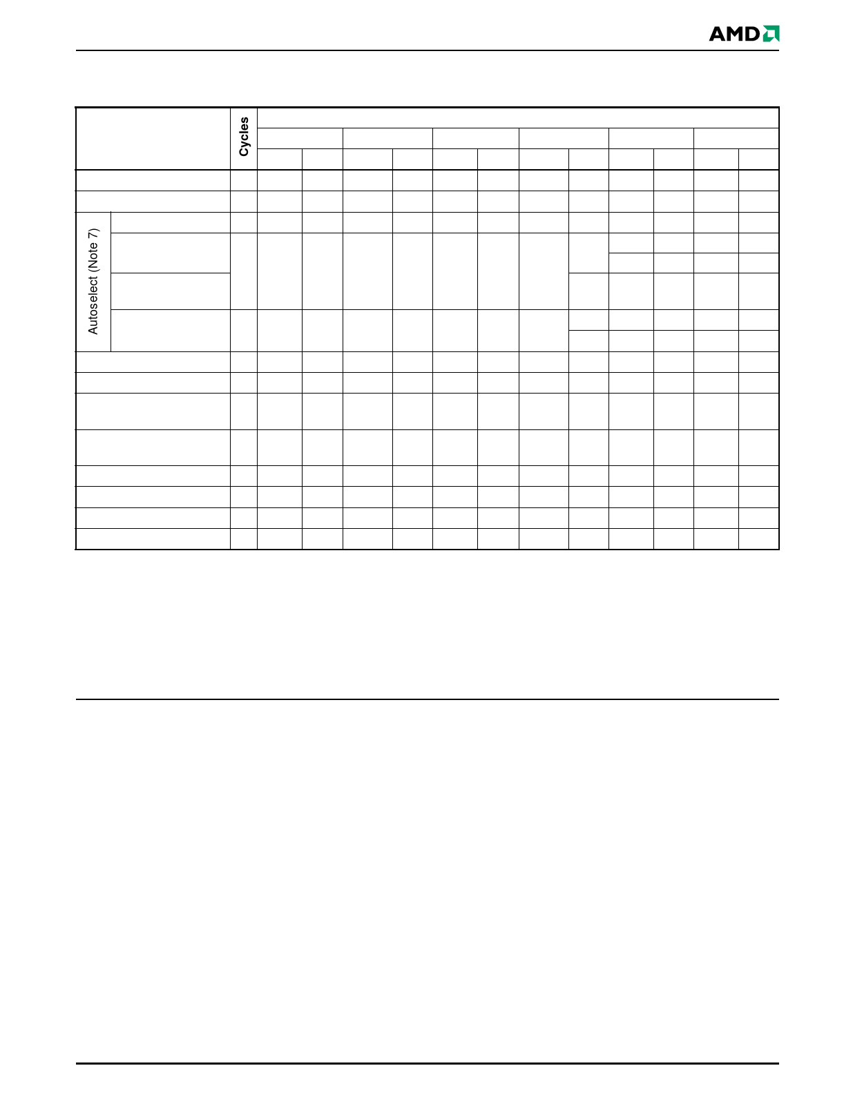
Command Definitions
Table 5. Am29LV001B Command Definitions
Command Sequence
(Note 1)
First
Addr Data
Second
Addr Data
Bus Cycles (Notes 2–4)
Third
Fourth
Addr Data Addr Data
Fifth
Addr Data
Sixth
Addr Data
Read (Note 5)
1 RA RD
Reset (Note 6)
1 XXX F0
Manufacturer ID
4 555 AA 2AA 55 555 90 X00 01
Device ID, Top Boot
Block
ED
4 555 AA 2AA 55 555 90 X01
Device ID, Bottom
Boot Block
6D
Sector Protect
Verify (Note 8)
4 555 AA 2AA
55
555
90
SA
X02
00
01
Byte Program
4 555 AA 2AA 55 555 A0 PA PD
Unlock Bypass
3 555 AA 2AA 55 555 20
Unlock Bypass Program
(Note 9)
2 XXX A0
PA
PD
Unlock Bypass Reset
(Note 10)
2 XXX 90 XXX 00
Chip Erase
6 555 AA 2AA 55 555 80 555 AA 2AA 55 555 10
Sector Erase
6 555 AA 2AA 55 555 80 555 AA 2AA 55 SA 30
Erase Suspend (Note 11) 1 XXX B0
Erase Resume (Note 12) 1 XXX 30
Legend:
X = Don’t care
RA = Address of the memory location to be read.
RD = Data read from location RA during read operation.
PA = Address of the memory location to be programmed.
Addresses are latched on the falling edge of the WE# or CE#
pulse.
PD = Data to be programmed at location PA. Data is latched
on the rising edge of WE# or CE# pulse.
SA = Address of the sector to be erased or verified. Address
bits A16–A12 uniquely select any sector.
Notes:
1. See Table 1 for descriptions of bus operations.
2. All values are in hexadecimal.
3. Except when reading array or autoselect data, all bus
cycles are write operations.
4. Address bits A16–A11 are don’t care for unlock and
command cycles, unless SA or PA required.
5. No unlock or command cycles required when device is in
read mode.
6. The Reset command is required to return to the read
mode when the device is in the autoselect mode or if DQ5
goes high.
7. The fourth cycle of the autoselect command sequence is
a read cycle.
8. The data is 00h for an unprotected sector and 01h for a
protected sector. The complete bus address in the fourth
cycle is composed of the sector address (A16–A12),
A1 = 1, and A0 = 0.
9. The Unlock Bypass command is required prior to the
Unlock Bypass Program command.
10. The Unlock Bypass Reset command is required to return
to reading array data when the device is in the Unlock
Bypass mode.
11. The system may read and program functions in non-
erasing sectors, or enter the autoselect mode, when in
the Erase Suspend mode. The Erase Suspend command
is valid only during a sector erase operation.
12. The Erase Resume command is valid only during the
Erase Suspend mode.
13. See the “Erase and Programming Performance” Section
for more information.
September 26, 2002
Am29LV001B
17
Share Link: