74VCX163245GX 查看數據表(PDF) - Fairchild Semiconductor
零件编号
产品描述 (功能)
生产厂家
74VCX163245GX
Fairchild Semiconductor

74VCX163245GX Datasheet PDF : 9 Pages
| |||
VCX163245 Translator Power Up Sequence Recommendations
To guard against power up problems, some simple guide-
lines need to be adhered to. The VCX163245 is designed
so that the control pins (T/Rn, OEn) are supplied by VCCB.
Therefore the first recommendation is to begin by powering
up the control side of the device, VCCB. The OEn control
pins should be ramped with or ahead of VCCB, this will
guard against bus contentions and oscillations as all A Port
and B Port outputs will be disabled. To ensure the high
impedance state during power up or power down, OEn
should be tied to VCCB through a pull up resistor. The mini-
mum value of the resistor is determined by the current
sourcing capability of the driver. Second, the T/Rn control
pins should be placed at logic LOW (0V) level, this will
ensure that the B-side bus pins are configured as inputs to
help guard against bus contention and oscillations. B-side
Data Inputs should be driven to a valid logic level (0V or
VCCB), this will prevent excessive current draw and oscilla-
tions. VCCA can then be powered up after VCCB, however
VCCA must be greater than or equal to VCCB to ensure
proper device operation. Upon completion of these steps
the device can then be configured for the users desired
operation. Following these steps will help to prevent possi-
ble damage to the translator device as well as other system
components.
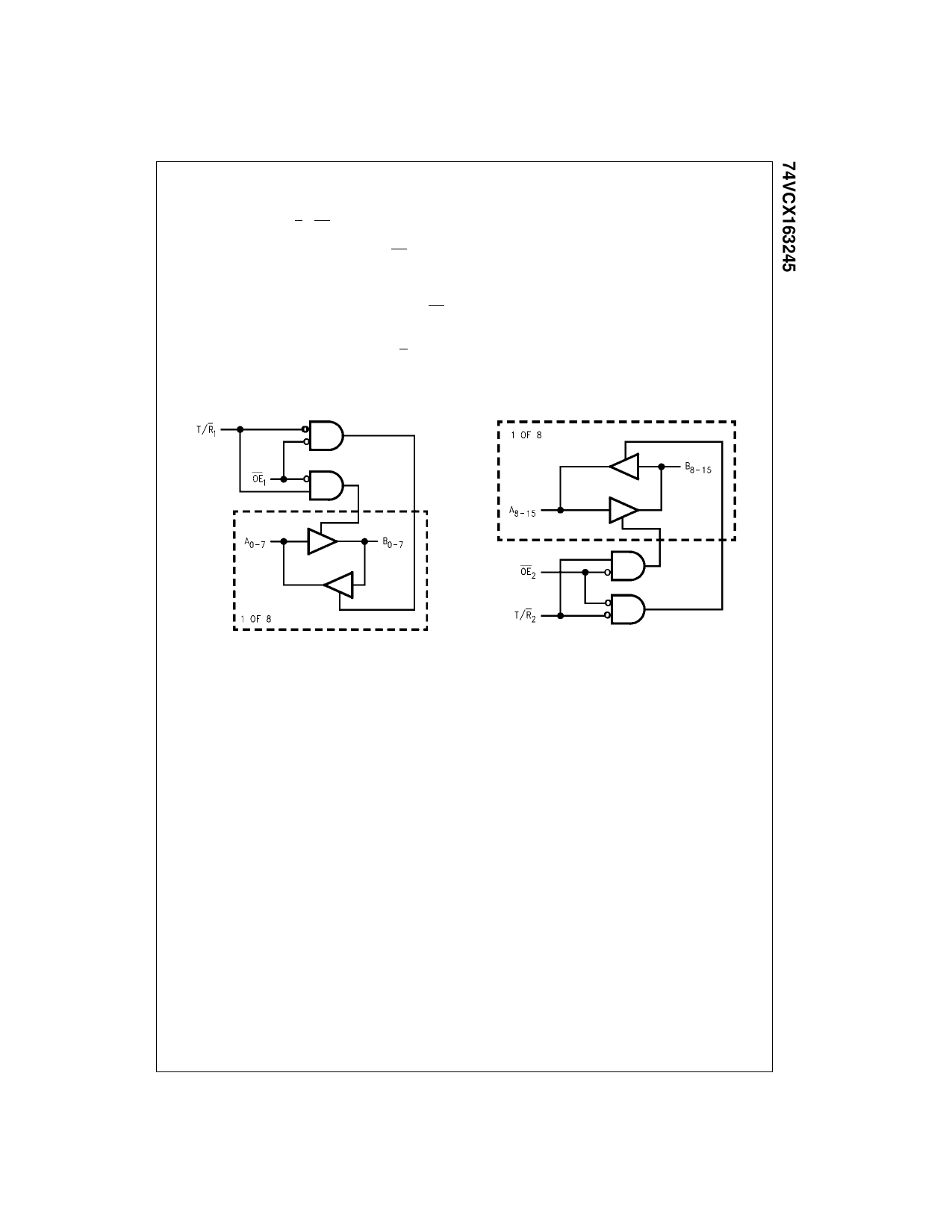
Logic Diagrams
Please note that these diagrams are provided only for the understanding of logic operations and should not be used to estimate propagation delays.
3
www.fairchildsemi.com
Share Link: