A25L10P 查看數據表(PDF) - AMIC Technology
零件编号
产品描述 (功能)
生产厂家
A25L10P
AMIC Technology

A25L10P Datasheet PDF : 43 Pages
| |||
A25L20P/A25L10P/A25L05P Series
INSTRUCTIONS
All instructions, addresses and data are shifted in and out of
the device, most significant bit first.
Serial Data Input (DIO) is sampled on the first rising edge of
Serial Clock (C) after Chip Select ( S ) is driven Low. Then, the
one-byte instruction code must be shifted in to the device,
most significant bit first, on Serial Data Input (DIO), each bit
being latched on the rising edges of Serial Clock (C).
The instruction set is listed in Table 5.
Every instruction sequence starts with a one-byte instruction
code. Depending on the instruction, this might be followed by
address bytes, or by data bytes, or by both or none.
In the case of a Read Data Bytes (READ), Read Data Bytes at
Higher Speed (Fast_Read), Read Status Register (RDSR) or
Release from Deep Power-down, Read Device Identification
and Read Electronic Signature (RES) instruction, the shifted-in
instruction sequence is followed by a data-out sequence. Chip
Select ( S ) can be driven High after any bit of the data-out
sequence is being shifted out.
In the case of a Page Program (PP), Sector Erase (SE), Bulk
Erase (BE), Write Status Register (WRSR), Write Enable
(WREN), Write Disable (WRDI) or Deep Power-down (DP)
instruction, Chip Select ( S ) must be driven High exactly at a
byte boundary, otherwise the instruction is rejected, and is not
executed. That is, Chip Select ( S ) must driven High when the
number of clock pulses after Chip Select ( S ) being driven Low
is an exact multiple of eight.
All attempts to access the memory array during a Write Status
Register cycle, Program cycle or Erase cycle are ignored, and
the internal Write Status Register cycle, Program cycle or
Erase cycle continues unaffected.
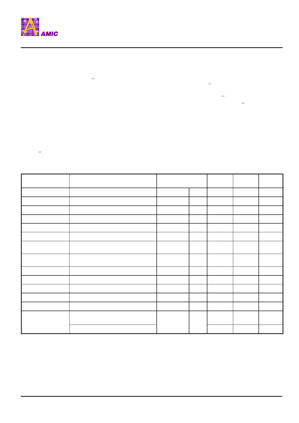
Table 5. Instruction Set
Instruction
Description
WREN
WRDI
RDSR
WRSR
READ
FAST_READ
FAST_READ_DUAL
_OUTPUT
FAST_READ_DUAL
_INPUT-OUTPUT
PP
SE
BE
DP
RDID
RES
Write Enable
Write Disable
Read Status Register
Write Status Register
Read Data Bytes
Read Data Bytes at Higher Speed
Read Data Bytes at Higher Speed by
Dual Output (1)
Read Data Bytes at Higher Speed by
Dual Input and Dual Output (1)
Page Program
Sector Erase
Bulk Erase
Deep Power-down
Read Device Identification
Release from Deep Power-down, and
Read Electronic Signature
Release from Deep Power-down
One-byte
Instruction Code
0000 0110 06h
0000 0100 04h
0000 0101 05h
0000 0001 01h
0000 0011 03h
0000 1011 0Bh
00111011 3Bh
10111011 BBh
0000 0010 02h
1101 1000 D8h
1100 0111 C7h
1011 1001 B9h
1001 1111 9Fh
1010 1011 ABh
Note: (1) DIO = (D6, D4, D2, D0)
DO = (D7, D5, D3, D1)
(2) Dual Input, DIO = (A22, A20, A18, ………, A6, A4, A2, A0)
DO = (A23, A21, A19, …….., A7, A5, A3, A1)
Address
Bytes
0
0
0
0
3
3
3
3(2)
3
3
0
0
0
0
0
Dummy
Bytes
0
0
0
0
0
1
1
1(2)
0
0
0
0
0
3
0
Data
Bytes
0
0
1 to ∞
1
1 to ∞
1 to ∞
1 to ∞
1 to ∞
1 to 256
0
0
0
1 to 4
1
0
(August, 2007, Version 1.0)
11
AMIC Technology Corp.
Share Link: