AD5245(Rev0) 查看數據表(PDF) - Analog Devices
零件编号
产品描述 (功能)
生产厂家
AD5245 Datasheet PDF : 16 Pages
| |||
AD5245
A repeated write function gives the user flexibility to update the
RDAC output a number of times after addressing and
instructing the part only once. During the write cycle, each data
byte will update the RDAC output. For example, after the RDAC
has acknowledged its slave address and instruction bytes, the
RDAC output will update after these two bytes. If another byte
is written to the RDAC while it is still addressed to a specific
slave device with the same instruction, this byte will update the
output of the selected slave device. If different instructions are
needed, the write mode has to start again with a new slave
address, instruction, and data byte. Similarly, a repeated read
function of the RDAC is also allowed.
Readback RDAC Value
The AD5245 allows the user to read back the RDAC values in
the read mode. Refer to Table 5 and Table 6 for the
programming format.
Multiple Devices on One Bus
Figure 40 shows two AD5245 devices on the same serial bus.
Each has a different slave address since the states of their AD0
pins are different. This allows each RDAC within each device to
be written to or read from independently. The master device
output bus line drivers are open-drain pull-downs in a fully I2C
compatible interface.
+5V
RP
RP
MASTER
+5V
SDA SCL
SDA SCL
SDA
SCL
AD0
AD5245
AD0
AD5245
Figure 40. Multiple AD5245 Devices on One I2C Bus
LEVEL SHIFTING FOR BIDIRECTIONAL INTERFACE
While most legacy systems may be operated at one voltage, a
new component may be optimized at another. When two
systems operate the same signal at two different voltages, proper
level shifting is needed. For instance, one can use a 3.3 V
E2PROM to interface with a 5 V digital potentiometer. A level
shifting scheme is needed to enable a bidirectional
communication so that the setting of the digital potentiometer
can be stored to and retrieved from the E2PROM. Figure 41
shows one of the implementations. M1 and M2 can be any
N-channel signal FETs, or if VDD falls below 2.5 V, low threshold
FETs such as the FDV301N.
VDD1 = 3.3V
RP
SDA1
SCL1
3.3V
RP
RP
G
S
D
G
M1
S
D
M2
VDD2 = 5V
RP
SDA2
SCL2
5V
E2PROM
AD5245
Figure 41. Level Shifting for Operation at Different Potentials
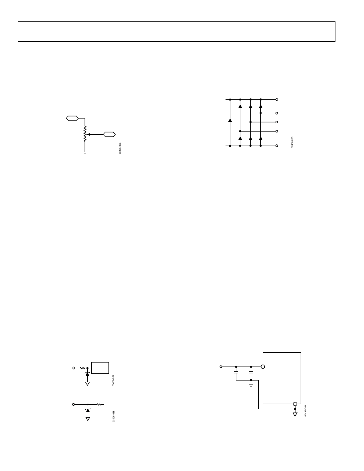
ESD PROTECTION
All digital inputs are protected with a series input resistor and
parallel Zener ESD structures shown in Figure 42 and Figure 43.
This applies to the digital input pins SDA, SCL, and AD0.
340Ω
LOGIC
VSS
Figure 42. ESD Protection of Digital Pins
A,B,W
VSS
Figure 43. ESD Protection of Resistor Terminals
TERMINAL VOLTAGE OPERATING RANGE
The AD5245 VDD and GND power supply defines the boundary
conditions for proper 3-terminal digital potentiometer
operation. Supply signals present on terminals A, B, and W that
exceed VDD or GND will be clamped by the internal forward
biased diodes (see Figure 44).
VDD
A
W
B
VSS
Figure 44. Maximum Terminal Voltages Set by VDD and VSS
Rev. 0 | Page 14 of 16
Share Link: 