5962-8853901EA(RevG) 查看數據表(PDF) - Analog Devices
零件编号
产品描述 (功能)
生产厂家
5962-8853901EA Datasheet PDF : 25 Pages
| |||
Data Sheet
AD524
THEORY OF OPERATION
The AD524 is a monolithic instrumentation amplifier based
on the classic 3-op amp circuit. The advantage of monolithic
construction is the closely matched components that enhance
the performance of the input preamplifier. The preamplifier
section develops the programmed gain by the use of feedback
concepts. The programmed gain is developed by varying the
value of RG (smaller values increase the gain) while the feedback
forces the collector currents (Q1, Q2, Q3, and Q4) to be constant,
which impresses the input voltage across RG.
As RG is reduced to increase the programmed gain, the
transconductance of the input preamplifier increases to the
transconductance of the input transistors. This has three
important advantages. First, this approach allows the circuit
to achieve a very high open-loop gain of 3 × 10⁸ at a programmed
gain of 1000, thus reducing gain-related errors to a negligible
30 ppm. Second, the gain bandwidth product, which is deter-
mined by C3 or C4 and the input transconductance, reaches
25 MHz. Third, the input voltage noise reduces to a value
determined by the collector current of the input transistors
for an RTI noise of 7 nV/√Hz at G = 1000.
INPUT PROTECTION
As interface amplifiers for data acquisition systems, instru-
mentation amplifiers are often subjected to input overloads,
that is, voltage levels in excess of the full scale for the selected
gain range. At low gains (10 or less), the gain resistor acts as a
current limiting element in series with the inputs. At high gains,
the lower value of RG does not adequately protect the inputs
from excessive currents. Standard practice is to place series
limiting resistors in each input, but to limit input current to
below 5 mA with a full differential overload (36 V) requires
over 7kΩ of resistance, which adds 10 nV√Hz of noise. To
provide both input protection and low noise, a special series
protection FET is used.
A unique FET design was used to provide a bidirectional
current limit, thereby protecting against both positive and
negative overloads. Under nonoverload conditions, three
channels (CH2, CH3, CH4) act as a resistance (≈1 kΩ) in series
with the input as before. During an overload in the positive
direction, a fourth channel, CH1, acts as a small resistance
(≈3 kΩ) in series with the gate, which draws only the leakage
current, and the FET limits IDSS. When the FET enhances under
a negative overload, the gate current must go through the small
FET formed by CH1 and when this FET goes into saturation,
the gate current is limited and the main FET goes into controlled
enhancement. The bidirectional limiting holds the maximum
input current to 3 mA over the 36 V range.
INPUT OFFSET AND OUTPUT OFFSET
Voltage offset specifications are often considered a figure of
merit for instrumentation amplifiers. While initial offset may
be adjusted to zero, shifts in offset voltage due to temperature
variations causes errors. Intelligent systems can often correct
this factor with an auto-zero cycle, but there are many small-
signal high-gain applications that do not have this capability.
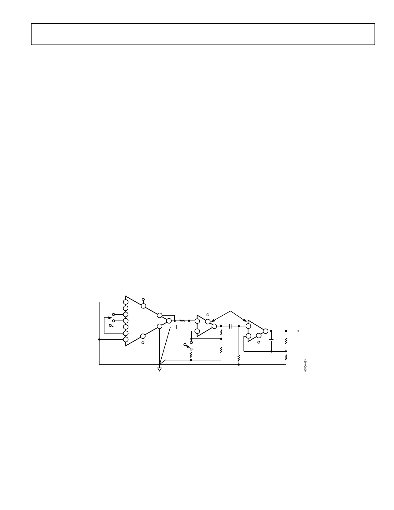
+VS
1–
16
10
13
100 12
8
AD524
10
16.2kΩ
9
+Vs
3+ 8
AD712
1µF
1000 11
6
1/2 1
RG2 3
1µF
2–
9.09kΩ
2+
7
G = 1, 10, 100
–VS
G = 1000
1kΩ
5+
1/2 7
6– 4
–VS
100Ω
1.62MΩ
1µF 16.2kΩ
1.82kΩ
Figure 33. Noise Test Circuit
Rev. G | Page 15 of 25
Share Link: 