AD524CDZ 查看數據表(PDF) - Analog Devices
零件编号
产品描述 (功能)
生产厂家
AD524CDZ Datasheet PDF : 28 Pages
| |||
AD524
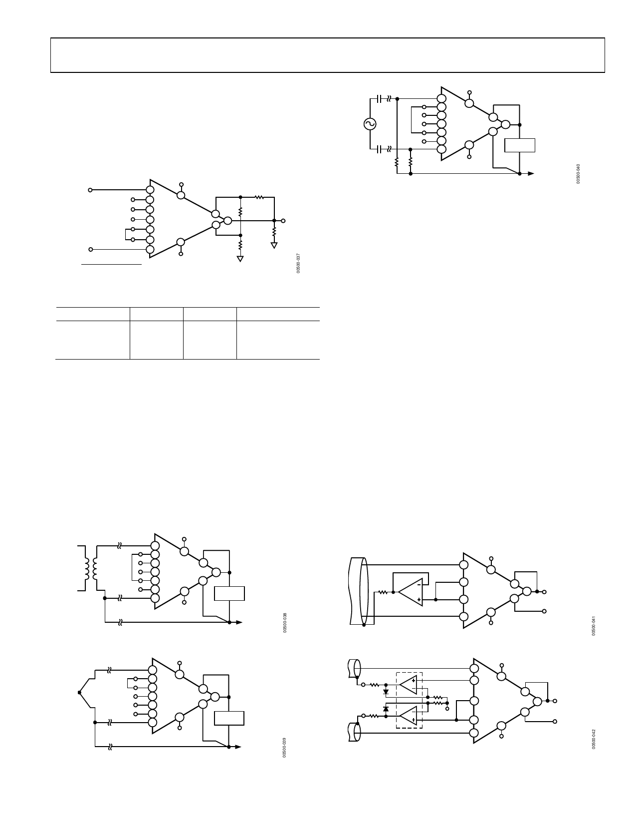
The AD524 can also be configured to provide gain in the output
stage. Figure 37 shows an H pad attenuator connected
to the reference and sense lines of the AD524. R1, R2, and R3
should be made as low as possible to minimize the gain variation
and reduction of CMRR. Varying R2 precisely sets the gain
without affecting CMRR. CMRR is determined by the match
of R1 and R3.
–INPUT
1
RG1
16
G = 10
13
G = 100
12
G = 1000
11
RG2
3
+INPUT
2
G = (R2||40kΩ) + R1 + R3
(R2||40kΩ)
+VS
8
AD524
7
–VS
R1
2.26kΩ
10
9
6
R2
5kΩ
R3
2.26kΩ
VOUT
RL
(R1 + R2 + R3)||RL ≥ 2kΩ
Figure 37. Gain of 2000
+VS
2+
8
3
11
12 AD524
13
16
1–
7
10
9
6
LOAD
–VS
TO POWER
SUPPLY
GROUND
Figure 40. Indirect Ground Returns for Bias Currents–AC-Coupled
Although instrumentation amplifiers have differential inputs,
there must be a return path for the bias currents. If this is not
provided, those currents charge stray capacitances, causing the
output to drift uncontrollably or to saturate. Therefore, when
amplifying floating input sources such as transformers and
thermocouples, as well as ac-coupled sources, there must still
be a dc path from each input to ground.
Table 4. Output Gain Resistor Values
Output Gain R2
R1, R3
2
5 kΩ
2.26 kΩ
5
1.05 kΩ 2.05 kΩ
10
1 kΩ
4.42 kΩ
Nominal Gain
2.02
5.01
10.1
INPUT BIAS CURRENTS
Input bias currents are those currents necessary to bias the
input transistors of a dc amplifier. Bias currents are an
additional source of input error and must be considered in
a total error budget. The bias currents, when multiplied by
the source resistance, appear as an offset voltage. What is of
concern in calculating bias current errors is the change in bias
current with respect to signal voltage and temperature. Input
offset current is the difference between the two input bias
currents. The effect of offset current is an input offset voltage
whose magnitude is the offset current times the source
impedance imbalance.
+VS
2+
3
8
11
10
12 AD524
9
13
6
16
7
1–
LOAD
–VS
TO POWER
SUPPLY
GROUND
Figure 38. Indirect Ground Returns for Bias Currents—Transformer Coupled
+VS
2+
8
3
11
12 AD524
13
16
1–
7
10
9
6
LOAD
–VS
TO POWER
SUPPLY
GROUND
Figure 39. Indirect Ground Returns for Bias Currents—Thermocouple
COMMON-MODE REJECTION
Common-mode rejection is a measure of the change in output
voltage when both inputs are changed equal amounts. These
specifications are usually given for a full-range input voltage
change and a specified source imbalance. Common-mode
rejection ratio (CMRR) is a ratio expression whereas common-
mode rejection (CMR) is the logarithm of that ratio. For
example, a CMRR of 10,000 corresponds to a CMR of 80 dB.
In an instrumentation amplifier, ac common-mode rejection is
only as good as the differential phase shift. Degradation of ac
common-mode rejection is caused by unequal drops across
differing track resistances and a differential phase shift due
to varied stray capacitances or cable capacitances. In many
applications, shielded cables are used to minimize noise. This
technique can create common-mode rejection errors unless the
shield is properly driven. Figure 41 and Figure 42 show active
data guards that are configured to improve ac common-mode
rejection by bootstrapping the capacitances of the input cabling,
thus minimizing differential phase shift.
100Ω
AD711
+VS
–INPUT 1 –
8
G = 100
12
RG2
AD524
3
+INPUT
2+
7
10
9
6
VOUT
REFERENCE
–VS
Figure 41. Shield Driver, G ≥ 100
100Ω
100Ω
–INPUT 1 –
+VS
AD712 RG1
8
16
10
12 AD524
9
–VS
3
RG2
6
7
2+
+INPUT
–VS
Figure 42. Differential Shield Driver
VOUT
REFERENCE
Rev. F | Page 17 of 28
Share Link: 