AD624 查看數據表(PDF) - Analog Devices
零件编号
产品描述 (功能)
生产厂家
AD624 Datasheet PDF : 17 Pages
| |||
AD624
50⍀
–IN
1
50⍀
+IN
2
3
INPUT
OFFSET
TRIM
4
20k⍀
VB
R1 5
10k⍀
10k⍀
6
10k⍀
–VS
+VS
1F C1 C2
35V
7
AD624
8
16
80.2⍀
15
4445.7⍀ 14
20k⍀
10k⍀
13
225.3⍀
12
124⍀
11
10k⍀
10
9
OUTPUT
OFFSET
TRIM
R2
10k⍀
G = 100 G = 200 G = 500
K1
K2
K3
NC
RELAY
SHIELDS
OUT
K1
K2
K3
D1
D2
D3
ANALOG
COMMON
K1 – K3 =
THERMOSEN DM2C
4.5V COIL
D1 – D3 = IN4148
INPUTS A
GAIN
Y0
RANGE B
GAIN TABLE
A B GAIN
74LS138
Y1
DECODER
Y2
0 0 100
0 1 500
1 0 200
11
1
+5V
7407N
BUFFER
DRIVER
+5V
10F
LOGIC
COMMON
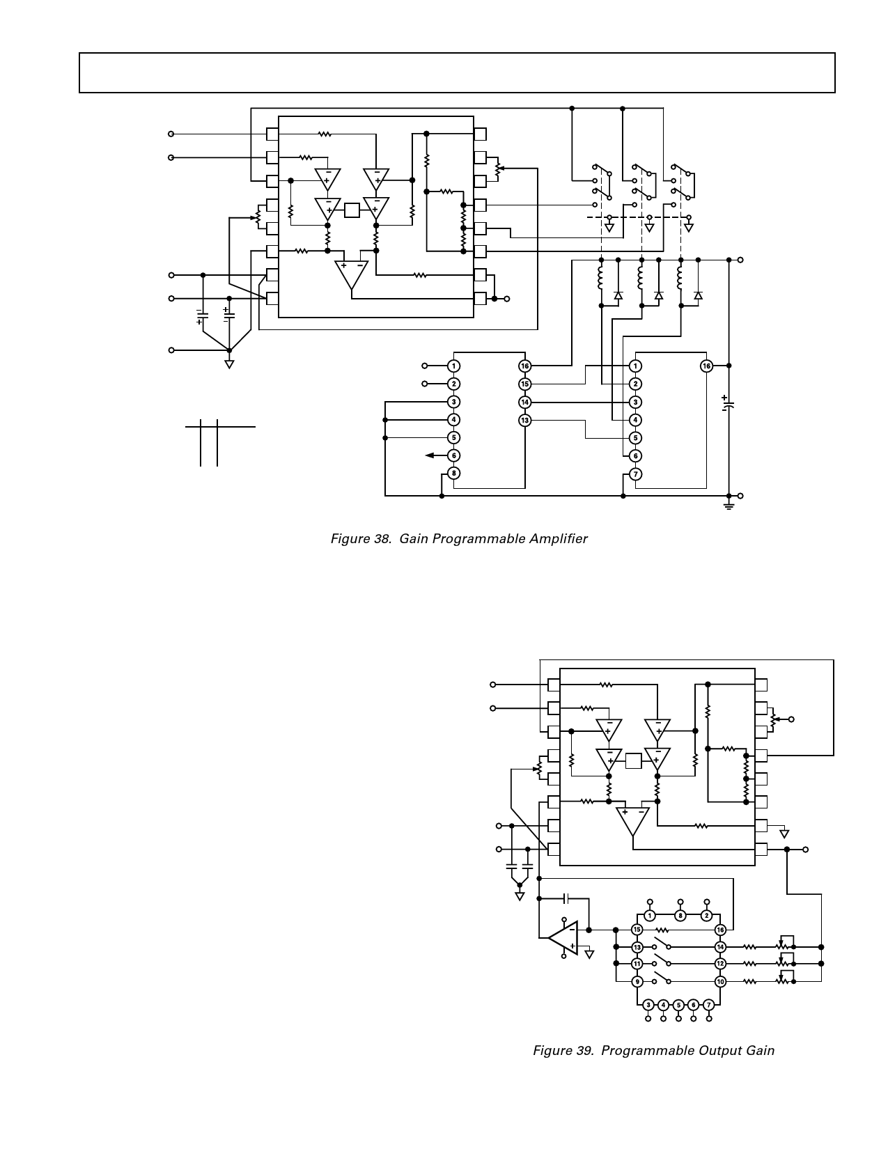
Figure 38. Gain Programmable Amplifier
By establishing a reference at the “low” side of a current setting
resistor, an output current may be defined as a function of input
voltage, gain and the value of that resistor. Since only a small
current is demanded at the input of the buffer amplifier A2, the
forced current IL will largely flow through the load. Offset and
drift specifications of A2 must be added to the output offset and
drift specifications of the IA.
PROGRAMMABLE GAIN
Figure 38 shows the AD624 being used as a software program-
mable gain amplifier. Gain switching can be accomplished with
mechanical switches such as DIP switches or reed relays. It
should be noted that the “on” resistance of the switch in series
with the internal gain resistor becomes part of the gain equation
and will have an effect on gain accuracy.
A significant advantage in using the internal gain resistors in a
programmable gain configuration is the minimization of thermo-
couple signals which are often present in multiplexed data
acquisition systems.
If the full performance of the AD624 is to be achieved, the user
must be extremely careful in designing and laying out his circuit
to minimize the remaining thermocouple signals.
The AD624 can also be connected for gain in the output stage.
Figure 39 shows an AD547 used as an active attenuator in the
output amplifier’s feedback loop. The active attenuation pre-
sents a very low impedance to the feedback resistors therefore
minimizing the common-mode rejection ratio degradation.
Another method for developing the switching scheme is to use a
DAC. The AD7528 dual DAC which acts essentially as a pair of
switched resistive attenuators having high analog linearity and
symmetrical bipolar transmission is ideal in this application. The
multiplying DAC’s advantage is that it can handle inputs of
either polarity or zero without affecting the programmed gain.
The circuit shown uses an AD7528 to set the gain (DAC A) and
to perform a fine adjustment (DAC B).
(+INPUT)
–IN
(–INPUT)
+IN
INPUT
OFFSET
NULL
10k⍀
–VS
+VS
1F
35V
50⍀
1
50⍀
2
3
4
20k⍀
VB
5
10k⍀
6
10k⍀
7
AD624
8
16
80.2⍀
15
14
4445.7⍀
20k⍀
10k⍀
13
225.3⍀
12
124⍀
11
10k⍀
10
OUTPUT
OFFSET
NULL
TO –V
10k⍀
9
VOUT
10pF
+VS
VSS VDD GND
AD711
–VS
AD7590
39.2k⍀
28.7k⍀
316k⍀
1k⍀
1k⍀
1k⍀
A1 A2 A3 A4 WR
Figure 39. Programmable Output Gain
REV. C
–11–
Share Link: 