AD8187 查看數據表(PDF) - Analog Devices
零件编号
产品描述 (功能)
生产厂家
AD8187 Datasheet PDF : 20 Pages
| |||
AD8186/AD8187
The AD8187
The AD8187 uses on-chip feedback resistors to realize the gain-
of-two function. To provide low crosstalk and a high output
impedance when disabled, each set of 500 Ω feedback resistors is
terminated by a dedicated reference buffer. A reference buffer is
a high speed op amp configured as a unity-gain follower. The
three reference buffers, one for each channel, share a single, high
impedance input, the VREF pin (see Figure 4). VREF input bias
current is typically less than 2 µA.
A0
B0
VREF
5V
5V
5V
GBUF 0
OUT 0
1؋
500⍀
500⍀
VFO
5V
GBUF 1
VF-1
500⍀ 500⍀
OUT1
VF-2
5V
GBUF 2
500⍀ 500⍀
OUT2
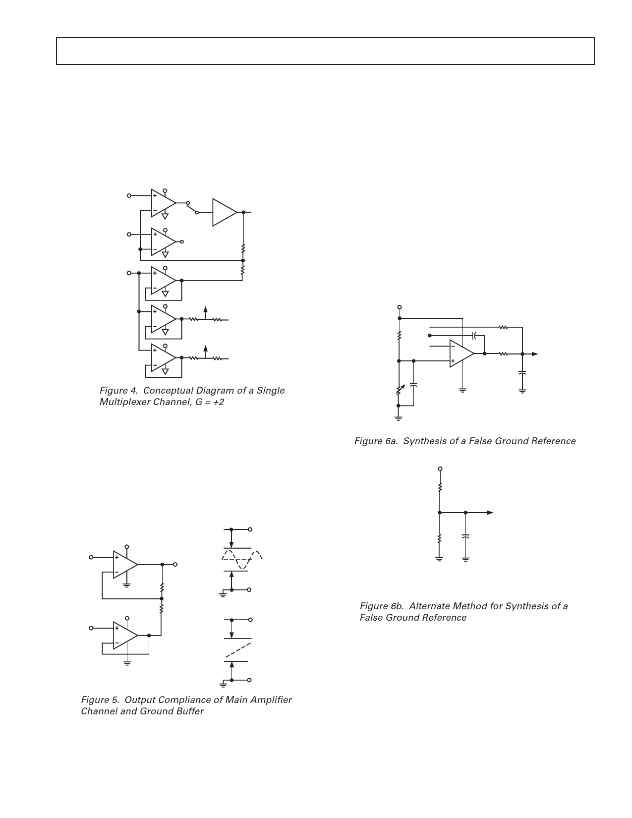
Figure 4. Conceptual Diagram of a Single
Multiplexer Channel, G = +2
This configuration has a few implications for single-supply
operation:
1) On the AD8187, VREF may not be tied to the most negative
analog supply, VEE.
Limits on Reference Voltage (AD8187, see Figure 5):
VEE + 1.3V < VREF < VCC – 1.6 V
1.3V < VREF < 3.4 V on 0 V /5 V Supplies
5V
A0
1.3V
OUT 0
1.3V
5V
VO_MAX = 3.7V
VOUT
VO_MIN = 1.3V
GND
5V
VREF
1.6V
1.3V
5V
VO_MAX = 3.4V
VREF
VO_MIN = 1.3V
GND
Figure 5. Output Compliance of Main Amplifier
Channel and Ground Buffer
2) Signal at the VREF pin appears at each output. Therefore,
VREF should be tied to a well bypassed, low impedance source.
Using superposition, it is easily shown that
VOUT = 2 × VIN – VREF
3) To maximize the output dynamic range, the reference voltage
should be chosen with some care.
For example, consider amplifying a 700 mV video signal with a
sync pulse 300 mV below black level. The user might decide to set
VREF at black level to preferentially run video signals on the faster
NPN transistor path. The AD8186 would, in this case, allow a
reference voltage as low as 1.3 V + 300 mV = 1.6 V. If the AD8187
is used, the sync pulse would be amplified to 600 mV. Therefore,
the lower limit on VREF becomes 1.3 V + 600 mV = 1.9 V. For
routing RGB video, an advantageous configuration would be to
employ +3 V and –2 V supplies, in which case VREF could be
tied to ground.
If system considerations prevent running the multiplexer on split
supplies, a false ground reference should be employed. A low
impedance reference may be synthesized with a second opera-
tional amplifier. Alternately, a well bypassed resistor divider
may serve. Refer to the Application section for further explana-
tion and more examples.
5V
100k⍀
1F
10k⍀
0.022F
OP21
100⍀
VREF
1F
GND
FROM 1992 ADI AMPLIFIER
APPLICATIONS GUIDE
Figure 6a. Synthesis of a False Ground Reference
5V
10k⍀
10k⍀
VREF
1F
CAP MUST BE LARGE
ENOUGH TO ABSORB
TRANSIENT CURRENTS
WITH MINIMUM BOUNCE.
Figure 6b. Alternate Method for Synthesis of a
False Ground Reference
High Impedance Disable
Both the AD8186 and the AD8187 may have their outputs
disabled to a high impedance state. In the case of the AD8187,
the reference buffers also disable to a state of high output
impedance. This feature prevents the feedback network of a
disabled channel from loading the output, which is valuable
when busing together the outputs of several muxes.
REV. A
–13–
Share Link: 