AD8225 查看數據表(PDF) - Analog Devices
零件编号
产品描述 (功能)
生产厂家
AD8225 Datasheet PDF : 16 Pages
| |||
AD8225
In the classical three op amp in amp topology shown in Figure 8,
gain is developed differentially between the two input amplifiers
A1 and A2, sacrificing CMV (common-mode voltage) range.
The gain of the in amp is typically 10 or less, and an additional
gain stage increases the overall gain to approximately 1000.
Gain developed in the input stage results in a trade-off in common-
mode voltage range, constraining the ability of the amplifier to
tolerate high dc electrode errors. Although the AD8225 is also
a three amplifier design, its gain of 5 is developed at the output
amplifier, improving the CMV range at the input. Using ± 5 V
supplies, the CMV range of the AD8225 is from –3.4 V to
+4 V, compared to –3.1 V to +3.8 V, a 7% improvement in
input headroom over conventional in amps with the same gain.
AD8225
G = 5 OP77
G = 200
100⍀ 19.6k⍀ 301⍀
AD8225
G = 5 OP77
G = 200
100⍀ 19.6k⍀ 301⍀
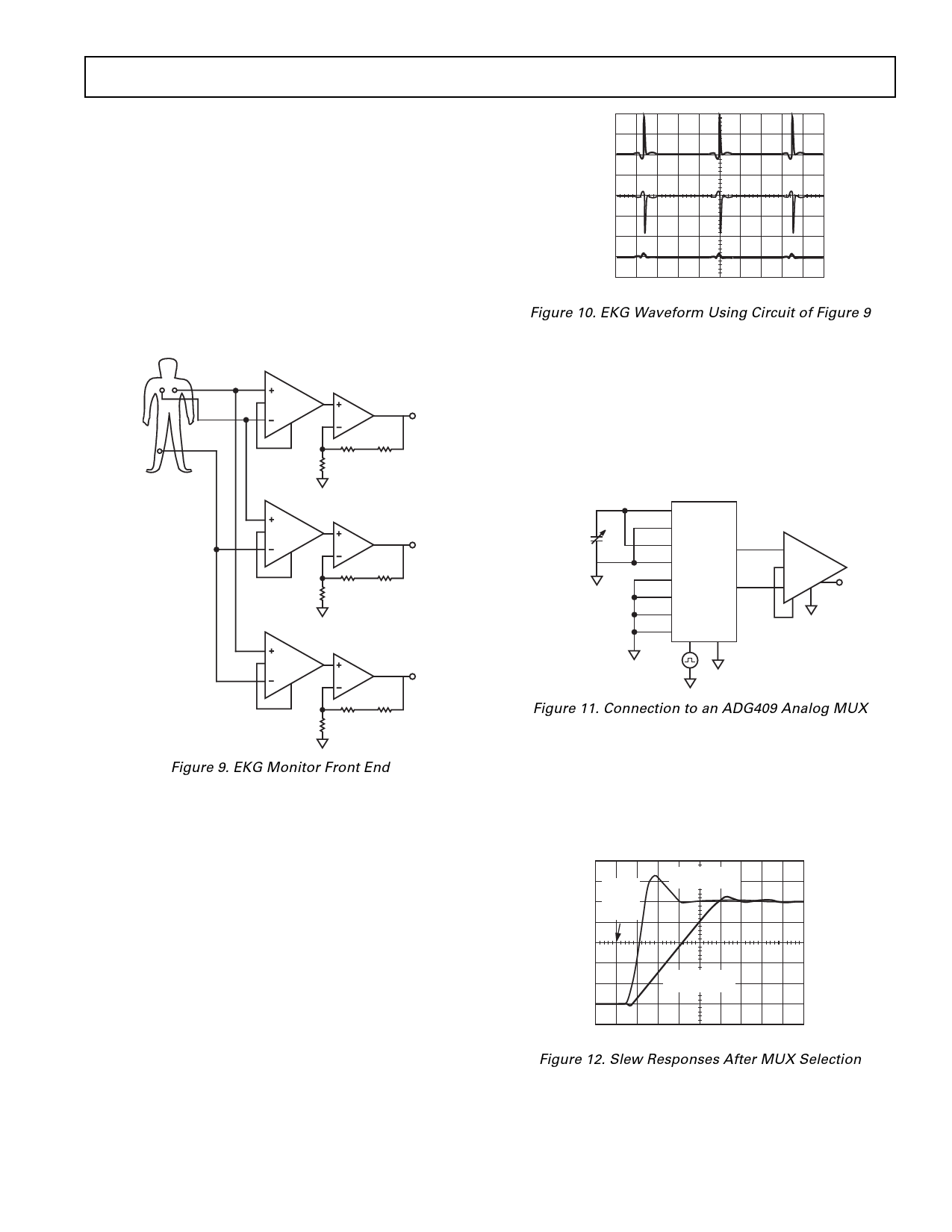
RA-LA 1
LA-LL 2
RA-LL 3
CH 1 = 2V, CH 2 = 2V, CH 3 = 2V, H = 200ms
Figure 10. EKG Waveform Using Circuit of Figure 9
Benefits of Fast Slew Rates
At 5 V/µs, the slew rate of the AD8225 is as fast as many op amp
circuits. This is an advantage in systems applications using multiple
sensors. For example, an analog multiplexer (see Figure 11) may
be used to select pairs of leads connected to several sensors. If
the AD8225 drives an ADC, the acquisition time is constrained
by the ability of the in amp to settle to a stable level after a new
set of leads is selected. Fast slew rates contribute greatly to
this function, especially if the difference in input levels is large.
0.2V, 2V
S1A
S1B
S2A
DA
S2B
S3A ADG409
1 AD8225
DB
S3B
REF
S4A
4
S4B
AD8225
G = 5 OP77
G = 200
100⍀ 19.6k⍀ 301⍀
Figure 9. EKG Monitor Front End
Figure 9 illustrates how an AD8225 may be used in an EKG
front end. In a low cost system, the AD8225 can be connected to
the patient. If buffers are required, the AD8225 can replace the
expensive precision resistor network and op amp.
Figure 10 shows test waveforms observed from the circuit of
Figure 9.
Figure 11. Connection to an ADG409 Analog MUX
Figure 12 illustrates the response of an AD8225 connected to
an ADG409 analog multiplexer in the circuit shown in Figure 11
at two signal levels. Two of the four MUX inputs are connected
to test dc levels. The remaining two are at ground potential so
that the output slews as the inputs A0 and A1 are addressed. As
can be seen, the output response settles well within 4 µs of the
applied level.
INPUT
SIGNAL
TRAN-
SITION
SMALL SIGNAL
(200mV/DIV)
LARGE SIGNAL
(2V/DIV)
CH 1 = 200mV, CH 2 = 2V, H = 500ns
Figure 12. Slew Responses After MUX Selection
REV. A
–13–
Share Link: 