ADM1028ARQ 查看數據表(PDF) - Analog Devices
零件编号
产品描述 (功能)
生产厂家
ADM1028ARQ Datasheet PDF : 16 Pages
| |||
ADM1028
Parameter
Min Typ Max
Unit Test Conditions
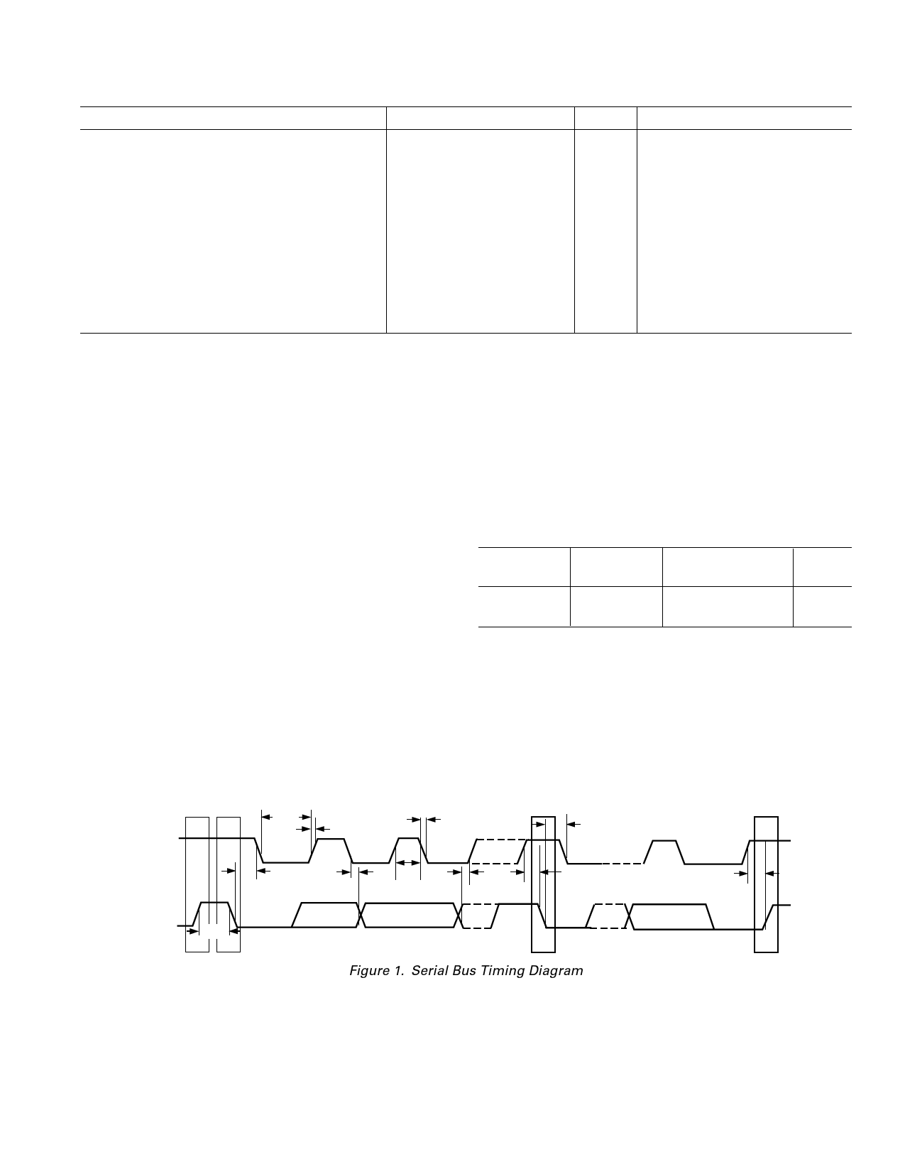
SERIAL BUS TIMING4
Clock Frequency, fSCLK
Bus Free Time, tBUF
Start Setup Time, tSU;STA
Start Hold Time, tHD;STA
Stop Condition Setup Time, tSU;STO
SCL Low Time, tLOW
SCL High Time, tHIGH
SCL, SDA Rise Time, tr
SCL, SDA Fall Time, tf
Data Setup Time, tSU;DAT
Data Hold Time, tHD;DAT
100
kHz See Figure 1
4.7
µs
See Figure 1
4.7
µs
See Figure 1
4.0
µs
See Figure 1
4.0
µs
See Figure 1
4.7
µs
See Figure 1
4.0
µs
See Figure 1
1000
ns
See Figure 1
300
ns
See Figure 1
250
ns
See Figure 1
300
ns
See Figure 1
NOTES
1Typicals are at TA = 25°C and represent most likely parametric norm. Standby current typ is measured with VCC = 3.3 V.
2Timing specifications are tested at logic levels of VIL = 0.8 V for a falling edge and VIH = 2.2 V for a rising edge.
3IOH for FAN_OFF guaranteed by design, not production tested.
4Guaranteed by design, not production tested.
Specifications subject to change without notice.
ABSOLUTE MAXIMUM RATINGS*
Positive Supply Voltage (VCC) . . . . . . . . . . . . . . . . . . . . . 6.5 V
Voltage on Digital Inputs Except Therm
and D– . . . . . . . . . . . . . . . . . . . . . . . . . . . . –0.3 V to +6.5 V
Voltage on Therm Pin . . . . . . . . . . . . . . –0.3 V to VCC + 0.3 V
Voltage on D– Pin . . . . . . . . . . . . . . . . . . . . –0.3 V to + 0.6 V
Voltage on Any Other Input . . . . . . . . . . –0.3 V to VCC + 0.3 V
or Output Pin
Input Current at Any Pin . . . . . . . . . . . . . . . . . . . . . . . ± 5 mA
Package Input Current . . . . . . . . . . . . . . . . . . . . . . . ± 20 mA
Maximum Junction Temperature (TJ max) . . . . . . . . . . 150°C
Storage Temperature Range . . . . . . . . . . . . –65°C to +150°C
Lead Temperatures
Soldering (10 sec) . . . . . . . . . . . . . . . . . . . . . . . . . . . 300°C
IR Reflow Peak Temperature . . . . . . . . . . . . . . . . . . . 220°C
ESD Rating (Human Body Model) . . . . . . . . . . . . . . . 4000 V
*Stresses above those listed under Absolute Maximum Ratings may cause perma-
nent damage to the device. This is a stress rating only; functional. Operation of the
device at these or any other conditions above those indicated in the operational
section of this specification is not implied. Exposure to absolute maximum rating
conditions for extended periods may affect device reliability.
THERMAL CHARACTERISTICS
16-Lead QSOP Package:
θJA = 105°C/W, θJC = 39°C/W
ORDERING GUIDE
Model
Temperature
Range
ADM1028ARQ 0°C to 100°C
Package
Description
Package
Option
Shrink Small Outline RQ-16
Package (QSOP)
SCL
tLOW
tR
tHD; STA
tHD; DAT
tF
tHIGH
tSU; DAT
tHD; STA
tSU; STA
tSU; STO
SDA
tBUF
P
S
S
P
Figure 1. Serial Bus Timing Diagram
REV. A
–3–
Share Link: 