ADM1060 查看數據表(PDF) - Analog Devices
零件编号
产品描述 (功能)
生产厂家
ADM1060 Datasheet PDF : 52 Pages
| |||
ADM1060
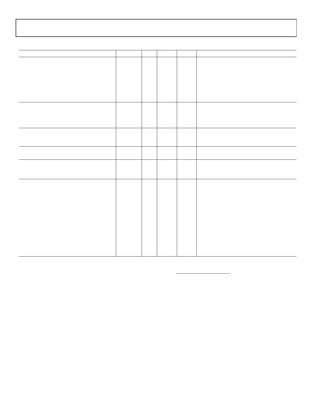
Parameter
Min
Typ Max Unit Test Conditions/Comments
DIGITAL INPUTS (GPI 1–4, WDI, A0, A1)4
Input High Voltage, VIH
2.0
V
Input Low Voltage, VIL
0.8
V
Input High Current, IIH
–1
µA
VIN = 5.5 V
Input Low Current, IIL
1
µA
VIN = 0 V
Input Capacitance
10
pF
Programmable Pull-Down Current, IPULLDOWN
10
µA
If known logic state required
SERIAL BUS DIGITAL INPUTS (SDA, SCL)
Input High Voltage, VIH
2.0
V
Input Low Voltage, VIL
0.8
V
Output Low Voltage, VOL
0.4
V
IOUT = −3.0 mA
PROGRAMMABLE DELAY BLOCK
Timeout
0
500
ms
16 programmable options on both rising and
falling edge
WATCHDOG TIMER INPUT
Timeout
0
12.8 s
Eight programmable timeout options
EEPROM RELIABILITY
Endurance5, 6
100
Kcycles
Data Retention7
10
Years
SERIAL BUS TIMING8
Clock Frequency, fSCLK
400
kHz
See Figure 27
Glitch Immunity, tSW
50
ns
See Figure 27
Bus Free Time, tBUF
4.7
µs
See Figure 27
Start Setup Time, tSU;STA
4.7
µs
See Figure 27
Start Hold Time, tHD;STA
4
µs
See Figure 27
SCL Low Time, tLOW
4.7
µs
See Figure 27
SCL High Time, tHIGH
4
µs
See Figure 27
SCL, SDA Rise Time, tr
1000 ns
See Figure 27
SCL, SDA Fall Time, tf
300
µs
See Figure 27
Data Setup Time, tSU;DAT
250
ns
See Figure 27
Data Hold Time, tHD;DAT
300
ns
See Figure 27
NOTES
1At least one VPn must be ≥3.0 V if used as supply. VH must be ≥4.5 V if used as supply.
2Specification is not production tested, but is supported by characterization data at initial product release.
31% threshold accuracy is only achievable on parts preprogrammed by Analog Devices. Contact ADM1060.program@analog.com for further details.
4Logic inputs will accept input high voltages up to 5.5 V even when the device is operating at supply voltages below 5 V.
5Endurance is qualified to 100,000 cycles as per JEDEC Std. 22 method A117, and measured at −40°C, +25°C, and +85°C.
6For programming and erasing of EEPROM, a minimum VDD = 3.0 V is required 0°C to +85°C and a minimum VDD = 4.5 V is required −40°C to 0°C.
7Retention lifetime equivalent at junction temperature (TJ) = 55°C as per JEDEC Std. 22 method A117.
8Timing specifications are tested at logic levels of VIL = 0.8 V for a falling edge and VIH = 2.0 V for a rising edge.
Rev. B | Page 6 of 52
Share Link: 