N28F001BN-B70 查看數據表(PDF) - Intel
零件编号
产品描述 (功能)
生产厂家
N28F001BN-B70 Datasheet PDF : 33 Pages
| |||
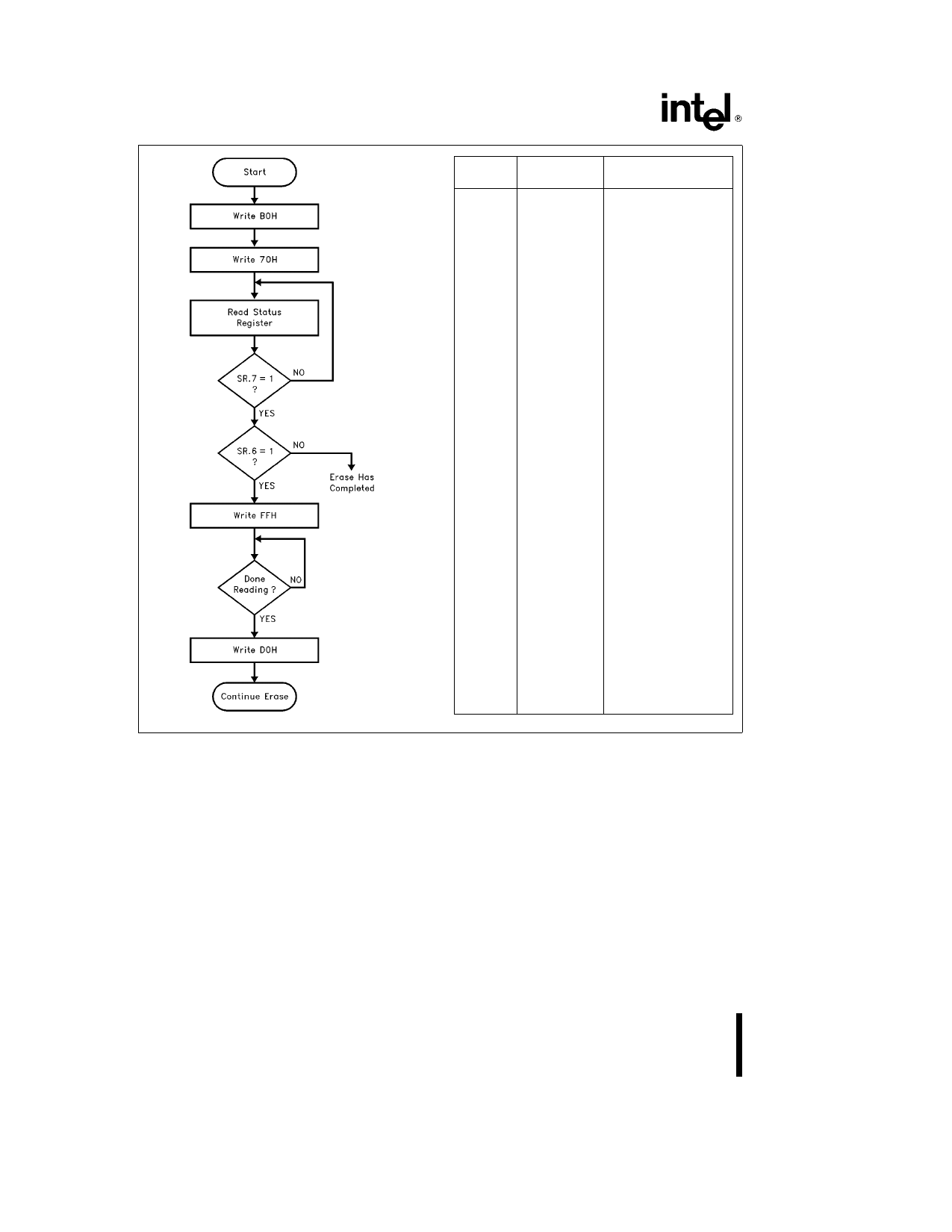
28F001BX-T 28F001BX-B
Bus
Operation
Command
Comments
Write
Erase
Suspend
Data e B0H
Write
Erase
Data e 70H
Status Register
Standby
Read
Read Status Register
Check SR 7
1 e Ready 0 e Busy
Toggle OE or CE to
Update Status Register
Standby
Check SR 6
1 e Suspended
Write
Read Array Data e FFH
Read
Read array data from
block other than that
being erased
Write Erase Resume Data e D0H
290406 – 9
Figure 11 28F001BX Erase Suspend Resume Flowchart
Programming Equipment
For PROM programming equipment that cannot
bring RP to high voltage OE provides an alter-
nate boot block access mechanism OE must tran-
sition to VHH a minimum of 480 ns before the initial
program erase setup command and held at VHH at
least 480 ns after program or erase confirm com-
mands are issued to the device After this interval
OE can return to normal TTL levels
DESIGN CONSIDERATIONS
Three-Line Output Control
Flash memories are often used in larger memory ar-
rays Intel provides three control inputs to accommo-
date multiple memory connections Three-line con-
trol provides for
a) lowest possible memory power dissipation
b) complete assurance that data bus contention will
not occur
To efficiently use these control inputs an address
decoder should enable CE while OE should be
connected to all memory devices and the system’s
READ control line This assures that only selected
memory devices have active outputs while deselect-
ed memory devices are in Standby Mode RP
should be connected to the system POWERGOOD
signal to prevent unintended writes during system
power transitions POWERGOOD should also toggle
during system reset
14
Share Link: 