GS8180D18D-250(2002) 查看數據表(PDF) - Giga Semiconductor
零件编号
产品描述 (功能)
生产厂家
GS8180D18D-250 Datasheet PDF : 27 Pages
| |||
Preliminary
GS8180D18D-333/300/250/200
JTAG Port Operation
Overview
The JTAG Port on this RAM operates in a manner that is compliant with IEEE Standard 1149.1-1990, a serial boundary scan interface standard
(commonly referred to as JTAG). The JTAG Port input interface levels scale with VDD. The JTAG output drivers are powered by VDD.
Disabling the JTAG Port
It is possible to use this device without utilizing the JTAG port. The port is reset at power-up and will remain inactive unless clocked. TCK, TDI,
and TMS are designed with internal pull-up circuits.To assure normal operation of the RAM with the JTAG Port unused, TCK, TDI, and TMS may
be left floating or tied to either VDD or VSS. TDO should be left unconnected.
JTAG Pin Descriptions
Pin
Pin Name I/O
Description
TCK
Test Clock
In
Clocks all TAP events. All inputs are captured on the rising edge of TCK and all outputs propagate
from the falling edge of TCK.
The TMS input is sampled on the rising edge of TCK. This is the command input for the TAP
TMS Test Mode Select In controller state machine. An undriven TMS input will produce the same result as a logic one input
level.
The TDI input is sampled on the rising edge of TCK. This is the input side of the serial registers
placed between TDI and TDO. The register placed between TDI and TDO is determined by the
TDI
Test Data In
In state of the TAP Controller state machine and the instruction that is currently loaded in the TAP
Instruction Register (refer to the TAP Controller State Diagram). An undriven TDI pin will produce
the same result as a logic one input level.
Output that is active depending on the state of the TAP state machine. Output changes in
TDO
Test Data Out
Out response to the falling edge of TCK. This is the output side of the serial registers placed between
TDI and TDO.
Note:
This device does not have a TRST (TAP Reset) pin. TRST is optional in IEEE 1149.1. The Test-Logic-Reset state is entered while TMS is
held high for five rising edges of TCK. The TAP Controller is also reset automatically at power-up.
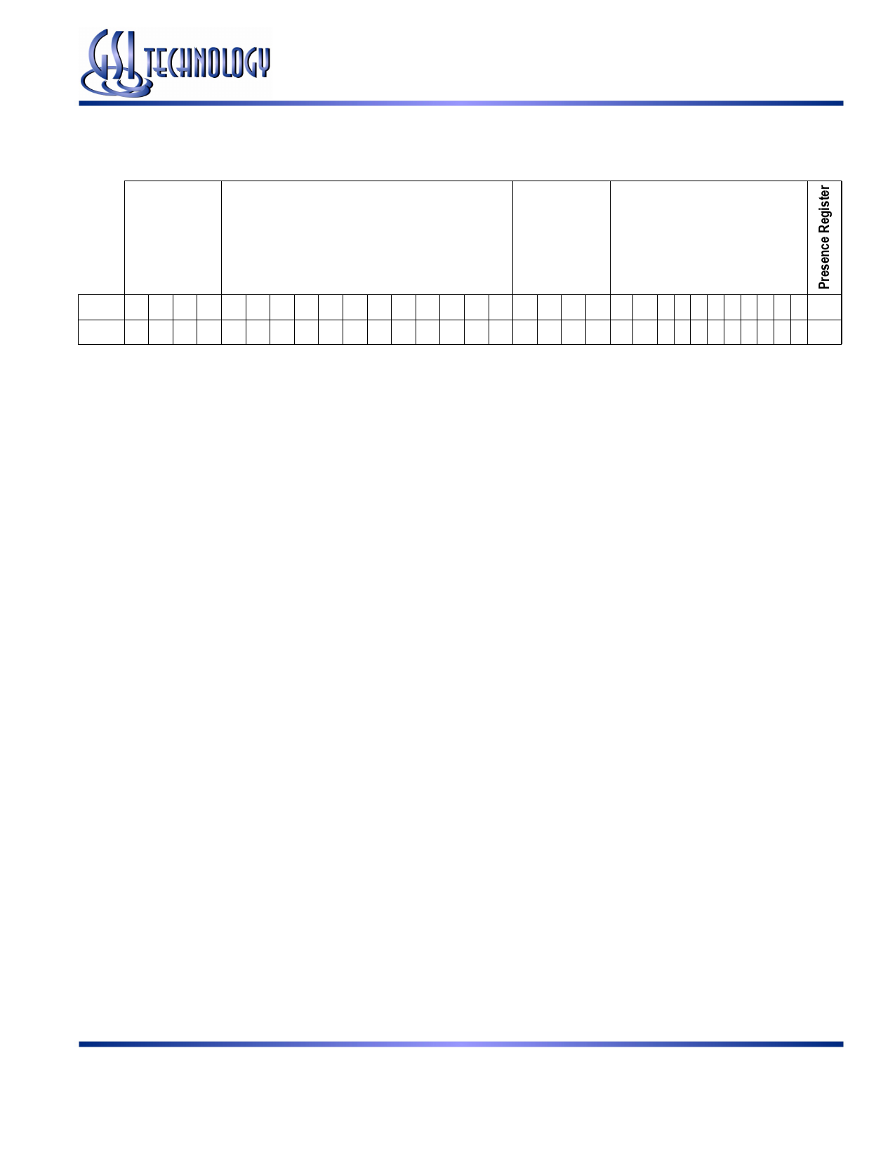
JTAG Port Registers
Overview
The various JTAG registers, referred to as Test Access Port or TAP Registers, are selected (one at a time) via the sequences of 1s and 0s
applied to TMS as TCK is strobed. Each of the TAP Registers is a serial shift register that captures serial input data on the rising edge of TCK
and pushes serial data out on the next falling edge of TCK. When a register is selected, it is placed between the TDI and TDO pins.
Instruction Register
The Instruction Register holds the instructions that are executed by the TAP controller when it is moved into the Run, Test/Idle, or the various
data register states. Instructions are 3 bits long. The Instruction Register can be loaded when it is placed between the TDI and TDO pins. The
Instruction Register is automatically preloaded with the IDCODE instruction at power-up or whenever the controller is placed in Test-Logic-Reset
state.
Bypass Register
The Bypass Register is a single bit register that can be placed between TDI and TDO. It allows serial test data to be passed through the RAM’s
JTAG Port to another device in the scan chain with as little delay as possible.
Rev: 2.00f 6/2002
21/27
© 2002, Giga Semiconductor, Inc.
Specifications cited are design targets and are subject to change without notice. For latest documentation contact your GSI representative.
Share Link: 