ARR01NBC 查看數據表(PDF) - Analog Devices
零件编号
产品描述 (功能)
生产厂家
ARR01NBC Datasheet PDF : 20 Pages
| |||
ADR01/ADR02/ADR03/ADR06
0.80
VIN = 15V
SAMPLE SIZE = 5
0.75
0.70
0.65
0.60
0.55
∆VTEMP/∆T 1.96mV/oC
0.50
0.45
0.40
–50 –25
0
25
50
75
TEMPERATURE (oC)
100 125
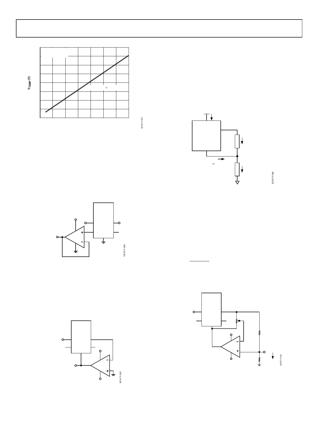
Figure 37. Voltage at TEMP Pin vs. Temperature
The TEMP function is provided as a convenience rather than a
precise feature. Because the voltage at the TEMP node is
acquired from the band gap core, current pulling from this pin
has a significant effect on VOUT. Care must be taken to buffer the
TEMP output with a suitable low bias current op amp, such as
the AD8601, AD820, or OP1177, all of which would result in
less than a 100 µV change in ∆VOUT (see Figure 38). Without
buffering, even tens of microamps drawn from the TEMP pin
can cause VOUT to fall out of specification.
15V
VIN
U1
ADR01/
ADR02/
ADR03/
ADR06
VIN VOUT
VO
VTEMP
1. 9mV/ oC
V+
OP1177
U2 V–
TEMP TRIM
GND
Figure 38. Temperature Monitoring
NEGATIVE REFERENCE
Without using any matching resistors, a negative reference can
be configured as shown in Figure 39. For the ADR01, the volt-
age difference between VOUT and GND is 10 V. Because VOUT is
at virtual ground, U2 closes the loop by forcing the GND pin to
be the negative reference node. U2 should be a precision op
amp with a low offset voltage characteristic.
5V TO 15V
U1
ADR01/
ADR02/
ADR03/
ADR06
VIN VOUT
TEMP TRIM
GND
+15V
–VREF
U2
V+
OP1177
V–
LOW COST CURRENT SOURCE
Unlike most references, the ADR01/ADR02/ADR03/ADR06
employ an NPN Darlington in which the quiescent current
remains constant with respect to the load current, as shown in
Figure 24. As a result, a current source can be configured as
shown in Figure 40 where ISET = (VOUT – VL)/RSET. IL is simply
the sum of ISET and IQ. Although simple, IQ varies typically from
0.55 to 0.65 mA, limiting this circuit to general-purpose
applications.
VIN
IIN
ADR01/
ADR02/
VOUT
ADR03/
ADR06
RSET
GND
IQ 0.6mA
RL
ISET = 10V/RSET
VL
IL = ISET + IQ
Figure 40. Low Cost Current Source
PRECISION CURRENT SOURCE WITH
ADJUSTABLE OUTPUT
A precision current source, on the other hand, can be
implemented with the circuit shown in Figure 41. By adding a
mechanical or digital potentiometer, this circuit becomes an
adjustable current source. If a digital potentiometer is used, the
load current is simply the voltage across terminals B to W of the
digital potentiometer divided by RSET.
IL
=
VREF × D
R SET
(1)
where D is the decimal equivalent of the digital potentiometer
input code.
+12V
U1
ADR01/
ADR02/
ADR03/
ADR06
VIN VOUT
TEMP TRIM
GND
0V TO (5V + VL)
B
AD5201 W
100kΩ
A
+12V
U2
V+
OP1177
–5V TO VL V–
RSET
1kΩ
VL
–12V
RL 1kΩ IL
Figure 41. Programmable 0 to 5 mA Current Source
–15V
Figure 39. Negative Reference
Rev. F | Page 16 of 20
Share Link: 