ATTL7582BC 查看數據表(PDF) - Agere -> LSI Corporation
零件编号
产品描述 (功能)
生产厂家
ATTL7582BC Datasheet PDF : 16 Pages
| |||

Data Sheet
November 1999
Application
L7582 Tip Ring Access Switch
TIP R1
SW5
LINE
TEST
ACCESS
CROWBAR
PROTECTION
R2
RING
SW6
LINE
TEST
ACCESS
SW3
RINGING
RETURN
SW1 BREAK
SW2 BREAK
SW4
RINGING
ACCESS
RING
GENERATOR
BATTERY
VBAT
REFERENCE
SCR
AND
TRIP
CKT
TIP
BATTERY
FEED
RING
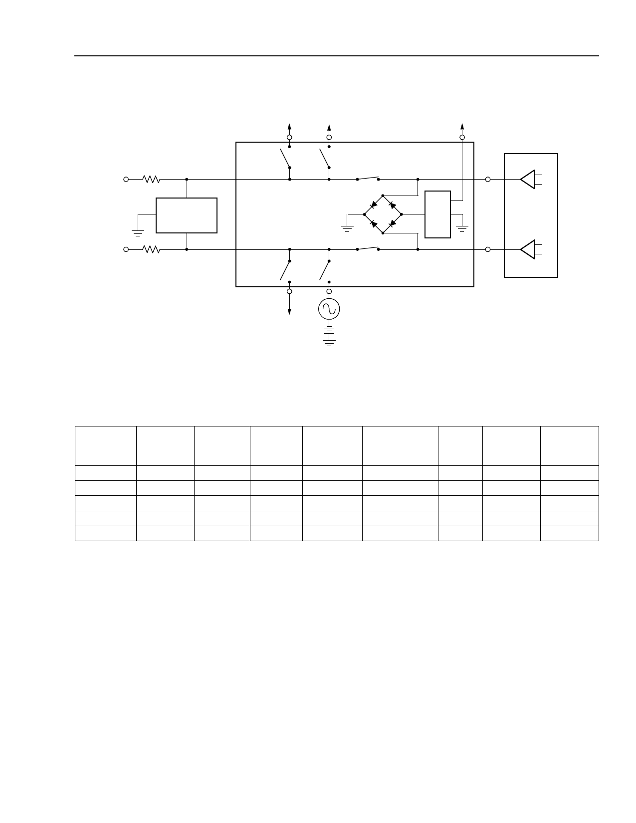
Figure 7. Typical TRAS Application, Idle, or Talk State Shown
12-2366.c (F)
Table 13. Truth Table
Input
Access
TSD
0V
5V
0V
5V
Don’t Care
0V
0V
5V
5V
Don’t Care
5 V/Float1
5 V/Float1
5 V/Float1
5 V/Float1
0 V2
Tip
Break
Switch
On
Off
Off
Off
Off
Ring
Break
Switch
On
Off
Off
Off
Off
Ringing
Return
Switch
Off
On
Off
Off
Off
Ring
Switch
Off
On
Off
Off
Off
Tip
Access
Switch
Off
Off
On
Off
Off
1. If TSD = 5 V, the thermal shutdown mechanism is disabled. If TSD is floating, the thermal shutdown mechanism is active.
2. Forcing TSD to ground overrides the logic input pins and forces an all OFF state.
3. Idle/Talk state.
4. Power ringing state.
5. Test out or message waiting state.
6. All OFF state.
Ring
Access
Switch
Off3
Off4
On5
Off6
Off6
A parallel in/parallel out data latch is integrated into the
L7582. Operation of the data latch is controlled by the
logic level input pin LATCH. The data input to the latch
is the INRING and INACCESS pins of the L7582, and the
output of the data latch is an internal node used for
state control.
When the LATCH control pin is at logic 0, the data latch
is transparent and data control signals flow directly
from INRING and INACCESS, through the data latch to
state control. Any changes in INRING and INACCESS will
be reflected in the state of the switches.
Lucent Technologies Inc.
When the LATCH control pin is at logic 1, the data latch
is active—the L7582 will no longer react to changes at
the INRING and INACCESS control pins. The state of the
switches is now latched; that is, the state of the
switches will remain as they were when the LATCH
input transitioned from logic 0 to logic 1. The switches
will not respond to changes in INRING and INACCESS as
long as LATCH is held high.
Note that the TSD input is not tied to the data latch. TSD
is not affected by the LATCH input. TSD input will over-
ride state control via INRING, INACCESS, and LATCH.
13