CAT25C33 查看數據表(PDF) - Catalyst Semiconductor => Onsemi
零件编号
产品描述 (功能)
生产厂家
CAT25C33 Datasheet PDF : 11 Pages
| |||
CAT25C33/65
directly to Vcc or tied to Vcc through a resistor. Figure lower half of the memory, the first page or the last page by
9 illustrates hold timing sequence.
setting these bits. Once protected the user may only
STATUS REGISTER
read from the protected portion of the array. These bits are
non-volatile.
The Status Register indicates the status of the device. The WPEN (Write Protect Enable) is an enable bit for the WP
The RDY (Ready) bit indicates whether the CAT25C33/
65 is busy with a write operation. When set to 1 a write
cycle is in progress and when set to 0 the device
indicates it is ready. This bit is read only.
The WEL (Write Enable) bit indicates the status of the
write enable latch . When set to 1, the device is in a
ts Write Enable state and when set to 0 the device is in
a Write Disable state. The WEL bit can only be set by
the WREN instruction and can be reset by the WRDI
r instruction.
a The BP0, BP1 and BP2 (Block Protect) bits indicate
which blocks are currently protected. These bits are
set by the user issuing the WRSR instruction. The user
P is allowed to protect any quarter of the memory, the
pin. The WP pin and WPEN bit in the status register control
the programmable hardware write protect feature.Hardware
write protection is enabled when WP is low and WPEN bit
is set to high. The user cannot write to the status register
(including the block protect bits and the WPEN bit) and the
block protected sections in thememory array when the chip
is hardware write protected. Only the sections of the
memory array that are not block protected can be written.
Hardware write protection is disabled when either WP pin is
high or the WPEN bit is zero.
DEVICE OPERATION
Write Enable and Disable
The CAT25C33/65 contains a write enable latch. This latch
must be set before any write operation. The device powers
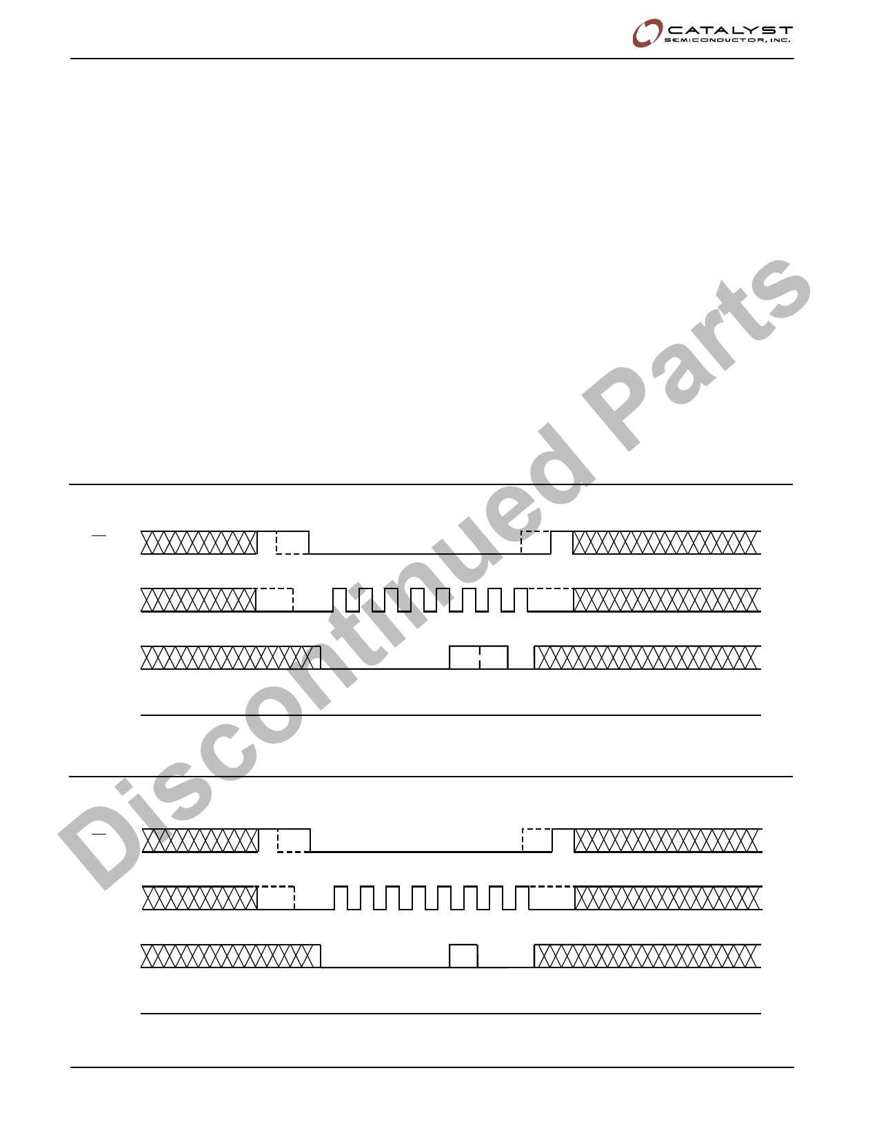
Figure 2. WREN Instruction Timing
d CS
ue SK
tin SI
0 0 0 0 0 1 10
HIGH IMPEDANCE
n SO
o Note: Dashed Line= mode (1, 1) — — — —
c Figure 3. WRDI Instruction Timing
Dis CS
SK
SI
0 0 0 0 0 1 00
SO
Note: Dashed Line= mode (1, 1) — — — —
HIGH IMPEDANCE
Doc. No. 1000, Rev. H
6
© 2005 by Catalyst Semiconductor, Inc.
Characteristics subject to change without notice
Share Link: 