A80960CF-33(2002) 查看數據表(PDF) - Intel
零件编号
产品描述 (功能)
生产厂家
A80960CF-33 Datasheet PDF : 70 Pages
| |||
80960-40, -33, -25
3.2
Pin Descriptions
This section defines the 80960CF pins. Table 2 presents the legend for interpreting the pin
descriptions in Tables 3 through 5. Table 3 presents the external bus signals. Table 4 presents
processor control signals. Table 5 presents the DMA and Interrupt Unit control signals.
Note: All pins float while the processor is in the ONCE mode.
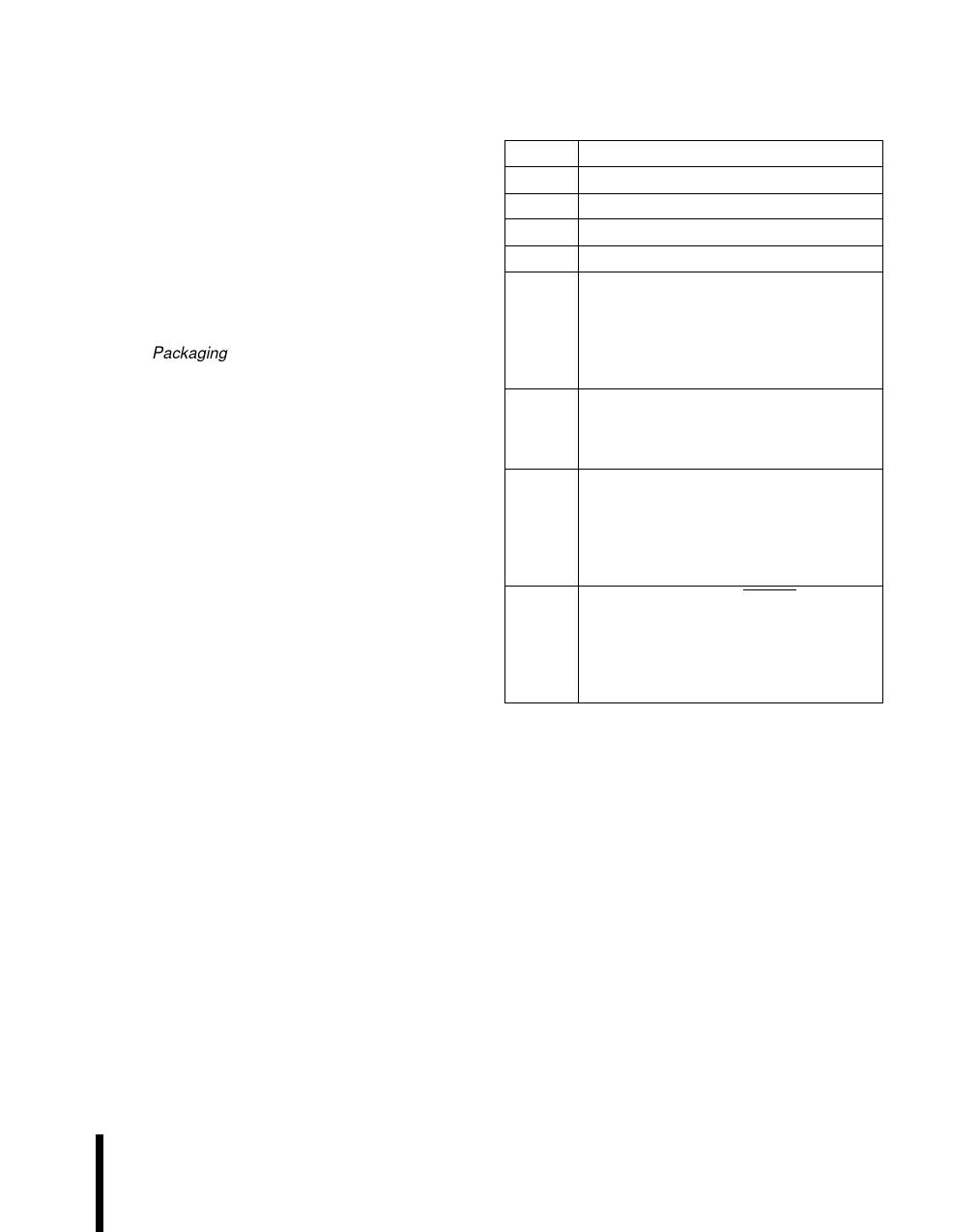
Table 2. Symbol Legend
Symbol
Description
I
O
I/O
–
S(...)
A(...)
H(...)
R(...)
Input only pin
Output only pin
Pin may be either an input or output
Pins “must be” connected as described
Synchronous. Inputs must meet setup and hold times relative to PCLK2:1 for proper operation.
Outputs are synchronous to PCLK2:1.
S(E) Edge sensitive input
S(L) Level sensitive input
Asynchronous. Inputs may be asynchronous to PCLK2:1.
A(E)Edge sensitive input
A(L)Level sensitive input
While the bus is in the Hold Acknowledge or Bus Backoff state, the pin:
H(1) is driven to VCC
H(0)is driven to VSS
H(Z) floats
H(Q)continues to be a valid input
While the processor’s RESET pin is low, the pin:
R(1) is driven to VCC
R(0)is driven to VSS
R(Z) floats
R(Q)continues to be a valid output
Datasheet
11
Share Link: 