DSPIC33FJ32GP204 查看數據表(PDF) - Microchip Technology
零件编号
产品描述 (功能)
生产厂家
DSPIC33FJ32GP204 Datasheet PDF : 284 Pages
| |||
dsPIC33FJ32GP202/204 and dsPIC33FJ16GP304
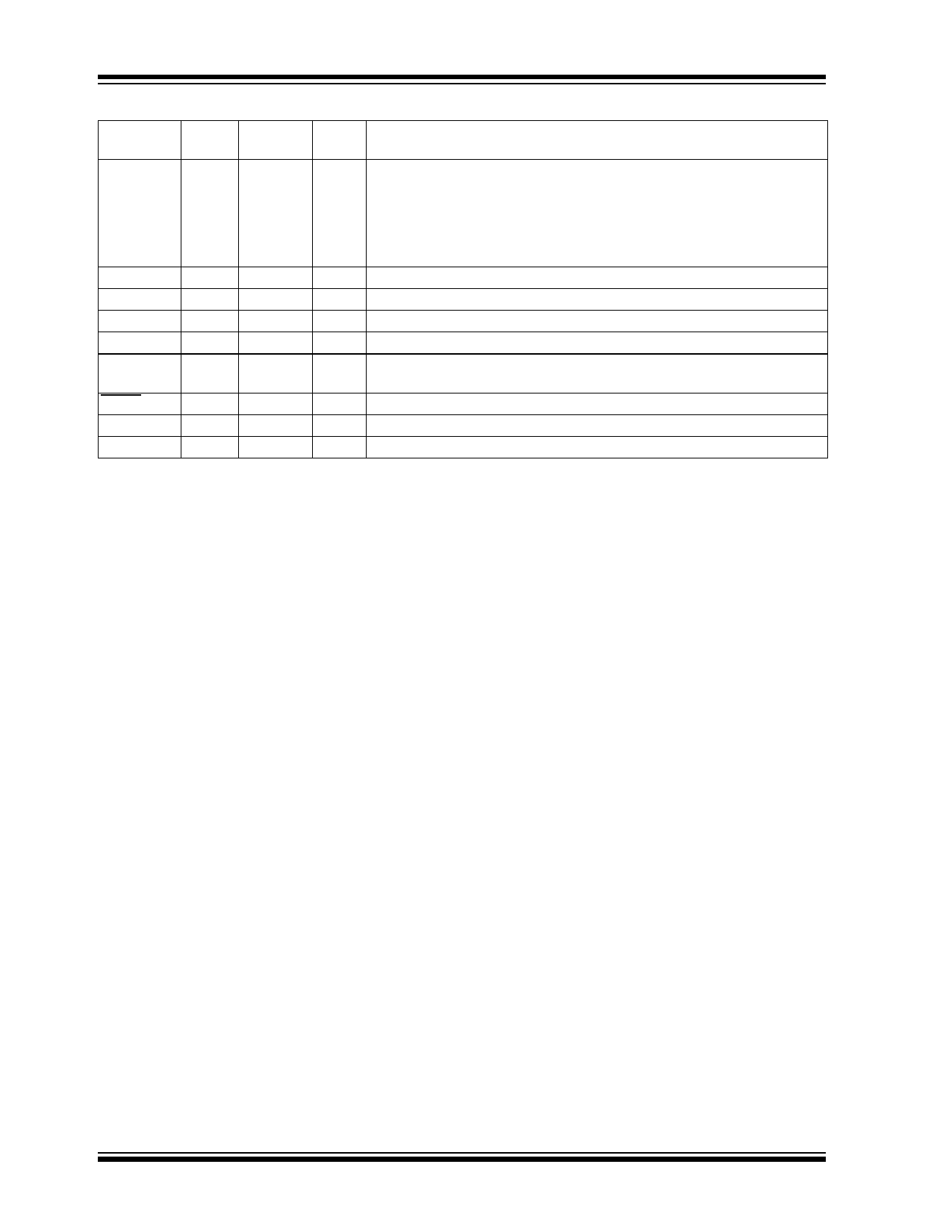
TABLE 1-1: PINOUT I/O DESCRIPTIONS (CONTINUED)
Pin Name
Pin
Type
Buffer
Type
PPS
Description
PGED1
PGEC1
PGED2
PGEC2
PGED3
PGEC3
I/O
ST
No Data I/O pin for programming/debugging communication channel 1.
I
ST
No Clock input pin for programming/debugging communication channel 1.
I/O
ST
No Data I/O pin for programming/debugging communication channel 2.
I
ST
No Clock input pin for programming/debugging communication channel 2.
I/O
ST
No Data I/O pin for programming/debugging communication channel 3.
I
ST
No Clock input pin for programming/debugging communication channel 3.
VCAP
P
—
No CPU logic filter capacitor connection.
VSS
P
—
No Ground reference for logic and I/O pins.
VREF+
I
Analog No Analog voltage reference (high) input.
VREF-
I
Analog No Analog voltage reference (low) input.
AVDD
P
P
No Positive supply for analog modules. This pin must be connected at all
times.
MCLR
I/P
ST
No Master Clear (Reset) input. This pin is an active-low Reset to the device.
Avss
P
P
No Ground reference for analog modules.
VDD
P
—
No Positive supply for peripheral logic and I/O pins.
Legend: CMOS = CMOS compatible input or output;
ST = Schmitt Trigger input with CMOS levels;
PPS = Peripheral Pin Select
Analog = Analog input; P = Power
O = Output;
I = Input
DS70290G-page 14
© 2011 Microchip Technology Inc.
Share Link: 