L7818CD2T-TR1 查看數據表(PDF) - STMicroelectronics
零件编号
产品描述 (功能)
生产厂家
L7818CD2T-TR1 Datasheet PDF : 52 Pages
| |||
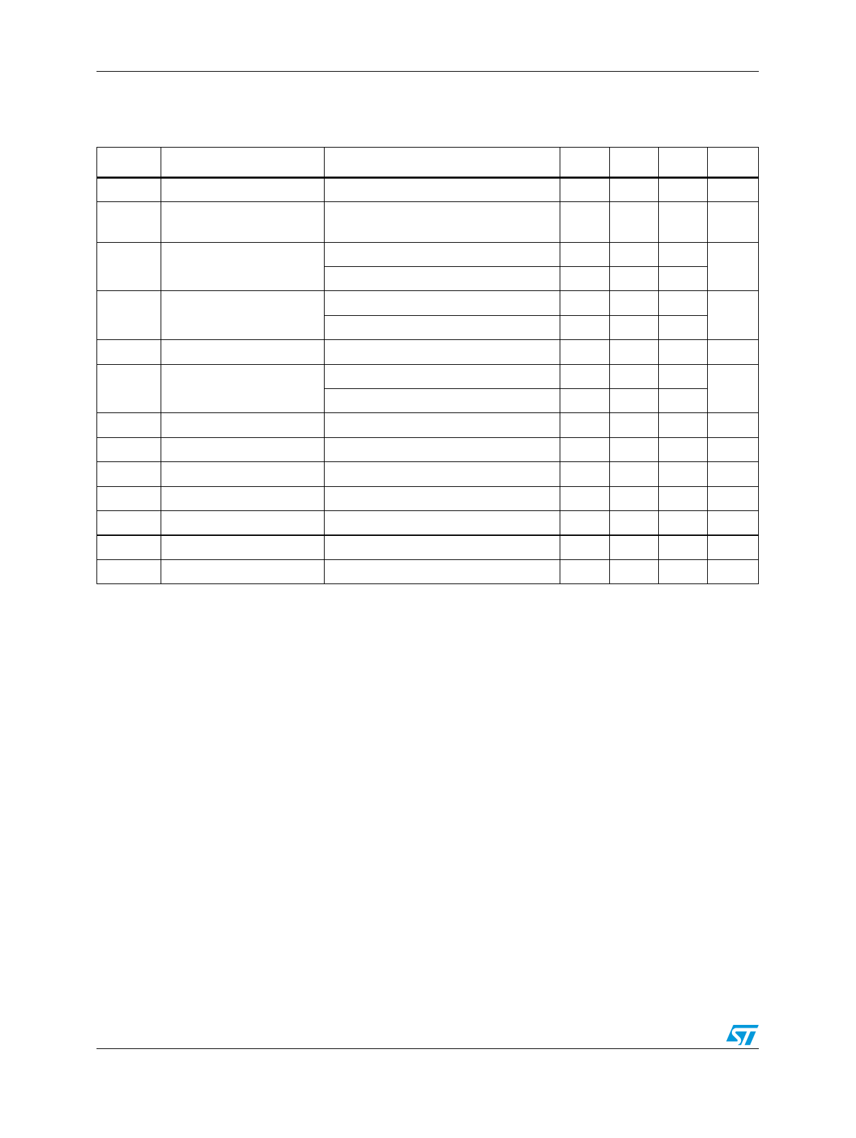
Electrical characteristics
L78xx - L78xxC
Table 9.
Symbol
Electrical characteristics of L7818 (refer to the test circuits, TJ = -55 to 150°C, VI = 26 V,
IO = 500 mA, CI = 0.33 µF, CO = 0.1 µF unless otherwise specified)
Parameter
Test conditions
Min. Typ. Max. Unit
VO Output voltage
TJ = 25°C
17.3 18 18.7 V
VO Output voltage
IO = 5 mA to 1 A, PO ≤15 W
VI = 22 to 33 V
17.1 18 18.9 V
ΔVO(1) Line regulation
VI = 21 to 33 V, TJ = 25°C
VI = 24 to 30 V, TJ = 25°C
180
mV
90
ΔVO(1) Load regulation
IO = 5 mA to 1.5 A, TJ = 25°C
IO = 250 to 750 mA, TJ = 25°C
180
mV
90
Id
Quiescent current
TJ = 25°C
6
mA
ΔId
IO = 5 mA to 1 A
Quiescent current change
VI = 22 to 33 V
0.5
mA
0.8
ΔVO/ΔT Output voltage drift
IO = 5 mA
2.3
mV/°C
eN Output noise voltage
B =10 Hz to 100 KHz, TJ = 25°C
40 µV/VO
SVR Supply voltage rejection VI = 22 to 32 V, f = 120 Hz
59
dB
Vd Dropout voltage
IO = 1 A, TJ = 25°C
2
2.5
V
RO Output resistance
f = 1 KHz
22
mΩ
Isc Short circuit current
VI = 35 V, TJ = 25°C
0.75 1.2
A
Iscp Short circuit peak current TJ = 25°C
1.3 2.2 3.3
A
1. Load and line regulation are specified at constant junction temperature. Changes in VO due to heating effects must be
taken into account separately. Pulse testing with low duty cycle is used.
16/52
Share Link: 