LT1374-5 查看數據表(PDF) - Linear Technology
零件编号
产品描述 (功能)
生产厂家
LT1374-5 Datasheet PDF : 28 Pages
| |||
LT1374
APPLICATIONS INFORMATION
WARNING! Peak voltage on the BOOST pin is the sum of
unregulated input voltage plus the voltage across the
boost capacitor. This normally means that peak BOOST
pin voltage is equal to input voltage plus output voltage,
but when the boost diode is connected to the regulator
input, peak BOOST pin voltage is equal to twice the input
voltage. Be sure that BOOST pin voltage does not exceed
its maximum rating.
For nearly all applications, a 0.27µF boost capacitor works
just fine, but for the curious, more details are provided
here. The size of the boost capacitor is determined by
switch drive current requirements. During switch on time,
drain current on the capacitor is approximately IOUT/ 50. At
peak load current of 4.25A, this gives a total drain of 85mA.
Capacitor ripple voltage is equal to the product of on time
and drain current divided by capacitor value;
∆V = (tON)(85mA/C). To keep capacitor ripple voltage to
less than 0.6V (a slightly arbitrary number) at the worst-
case condition of tON = 1.8µs, the capacitor needs to be
0.27µF. Boost capacitor ripple voltage is not a critical
parameter, but if the minimum voltage across the capaci-
tor drops to less than 3V, the power switch may not
saturate fully and efficiency will drop. An approximate
formula for absolute minimum capacitor value is:
( ( )( )( ) ) CMIN =
IOUT / 50 VOUT / VIN
f VOUT − 3V
f = Switching frequency
VOUT = Regulated output voltage
VIN = Minimum input voltage
This formula can yield capacitor values substantially less
than 0.27µF, but it should be used with caution since it
does not take into account secondary factors such as
capacitor series resistance, capacitance shift with tem-
perature and output overload.
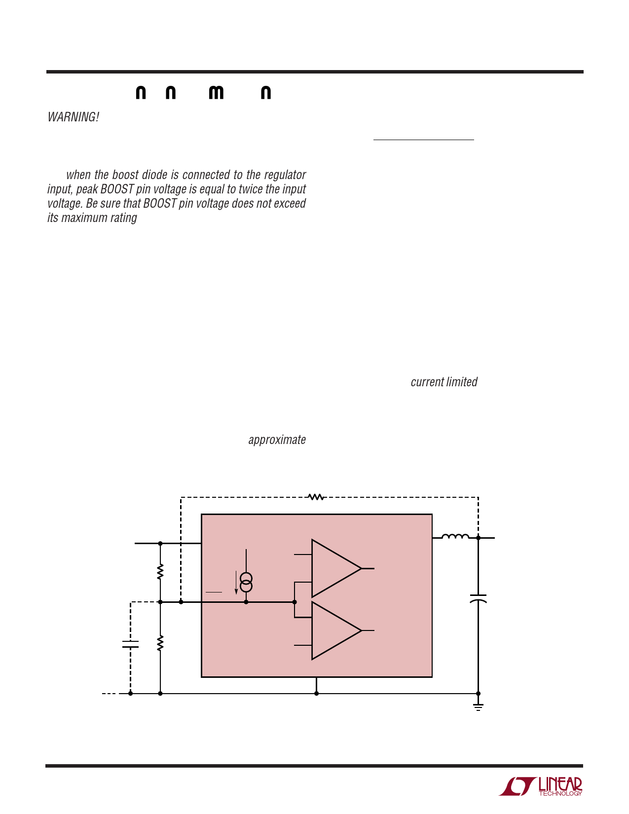
SHUTDOWN FUNCTION AND
UNDERVOLTAGE LOCKOUT
Figure 4 shows how to add undervoltage lockout (UVLO)
to the LT1374. Typically, UVLO is used in situations where
the input supply is current limited, or has a relatively high
source resistance. A switching regulator draws constant
power from the source, so source current increases as
source voltage drops. This looks like a negative resistance
load to the source and can cause the source to current limit
or latch low under low source voltage conditions. UVLO
RFB
INPUT
RHI
C1
RLO
LT1374
IN
SHDN
2.38V
+
3.5µA
–
+
0.4V
–
GND
VSW
STANDBY
TOTAL
SHUTDOWN
OUTPUT
+
1374 F04
Figure 4. Undervoltage Lockout
14
Share Link: 