LT1376 查看數據表(PDF) - Linear Technology
零件编号
产品描述 (功能)
生产厂家
LT1376 Datasheet PDF : 28 Pages
| |||
LT1375/LT1376
APPLICATIONS INFORMATION
POSITIVE-TO-NEGATIVE CONVERTER
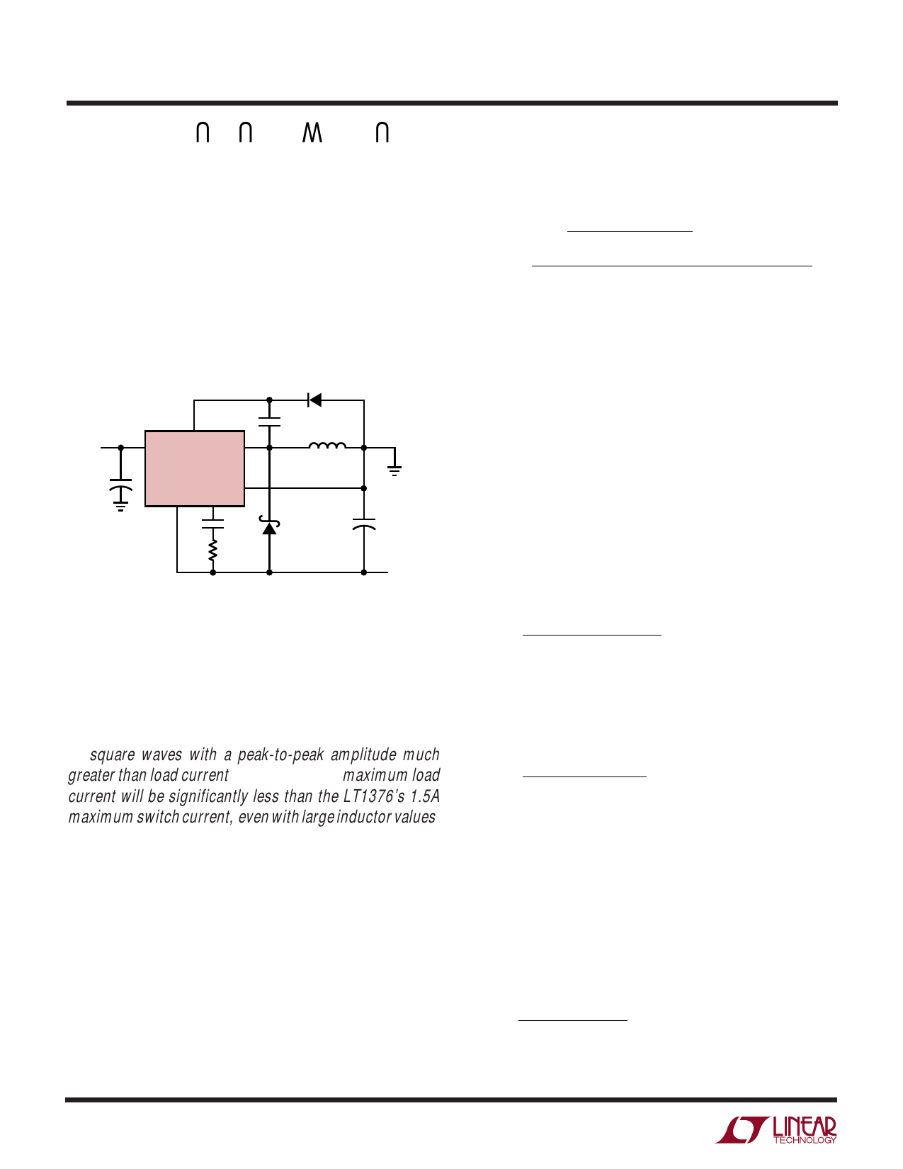
The circuit in Figure 18 is a classic positive-to-negative
topology using a grounded inductor. It differs from the
standard approach in the way the IC chip derives its
feedback signal, however, because the LT1376 accepts
only positive feedback signals, the ground pin must be tied
to the regulated negative output. A resistor divider to
ground or, in this case, the sense pin, then provides the
proper feedback voltage for the chip.
D1
1N4148
INPUT
4.5V TO
20V
C3 +
10µF TO
50µF
BOOST
VIN
VSW
LT1376-5
SENSE
GND VC
CC
C2
0.1µF L1*
5µH
D2
1N5818
+ C1
100µF
10V TANT
RC
OUTPUT**
–5V, 0.5A
* INCREASE L1 TO 10µH OR 20µH FOR HIGHER CURRENT APPLICATIONS.
SEE APPLICATIONS INFORMATION
** MAXIMUM LOAD CURRENT DEPENDS ON MINIMUM INPUT VOLTAGE
AND INDUCTOR SIZE. SEE APPLICATIONS INFORMATION
1375/76 F18
Figure 18. Positive-to-Negative Converter
Inverting regulators differ from buck regulators in the
basic switching network. Current is delivered to the output
as square waves with a peak-to-peak amplitude much
greater than load current. This means that maximum load
current will be significantly less than the LT1376’s 1.5A
maximum switch current, even with large inductor values.
The buck converter in comparison, delivers current to the
output as a triangular wave superimposed on a DC level
equal to load current, and load current can approach 1.5A
with large inductors. Output ripple voltage for the positive-
to-negative converter will be much higher than a buck
converter. Ripple current in the output capacitor will also
be much higher. The following equations can be used to
calculate operating conditions for the positive-to-negative
converter.
Maximum load current:
(( ( )( )())( ))(( )( ) ) IMAX
=
IP
−
2
VIN VOUT
VOUT + VIN f L
VOUT + VIN − 0.5
VOUT
VOUT +
VIN
VF
−
0.5
IP = Maximum rated switch current
VIN = Minimum input voltage
VOUT = Output voltage
VF = Catch diode forward voltage
0.5 = Switch voltage drop at 1.5A
Example: with VIN(MIN) = 4.7V, VOUT = 5V, L = 10µH, VF =
0.5V, IP = 1.5A: IMAX = 0.52A. Note that this equation does
not take into account that maximum rated switch current
(IP) on the LT1376 is reduced slightly for duty cycles
above 50%. If duty cycle is expected to exceed 50% (input
voltage less than output voltage), use the actual IP value
from the Electrical Characteristics table.
Operating duty cycle:
DC =
VOUT + VF
VIN − 0.3 + VOUT + VF
(This formula uses an average value for switch loss, so it
may be several percent in error.)
With the conditions above:
DC =
5 + 0.5
= 56%
4.7 − 0.3 + 5 + 0.5
This duty cycle is close enough to 50% that IP can be
assumed to be 1.5A.
OUTPUT DIVIDER
If the adjustable part is used, the resistor connected to
VOUT (R2) should be set to approximately 5k. R1 is
calculated from:
( ) R1= R2 VOUT − 2.42
2.42
24
Share Link: 