1506F 查看數據表(PDF) - Linear Technology
零件编号
产品描述 (功能)
生产厂家
1506F Datasheet PDF : 24 Pages
| |||
LT1506
APPLICATIONS INFORMATION
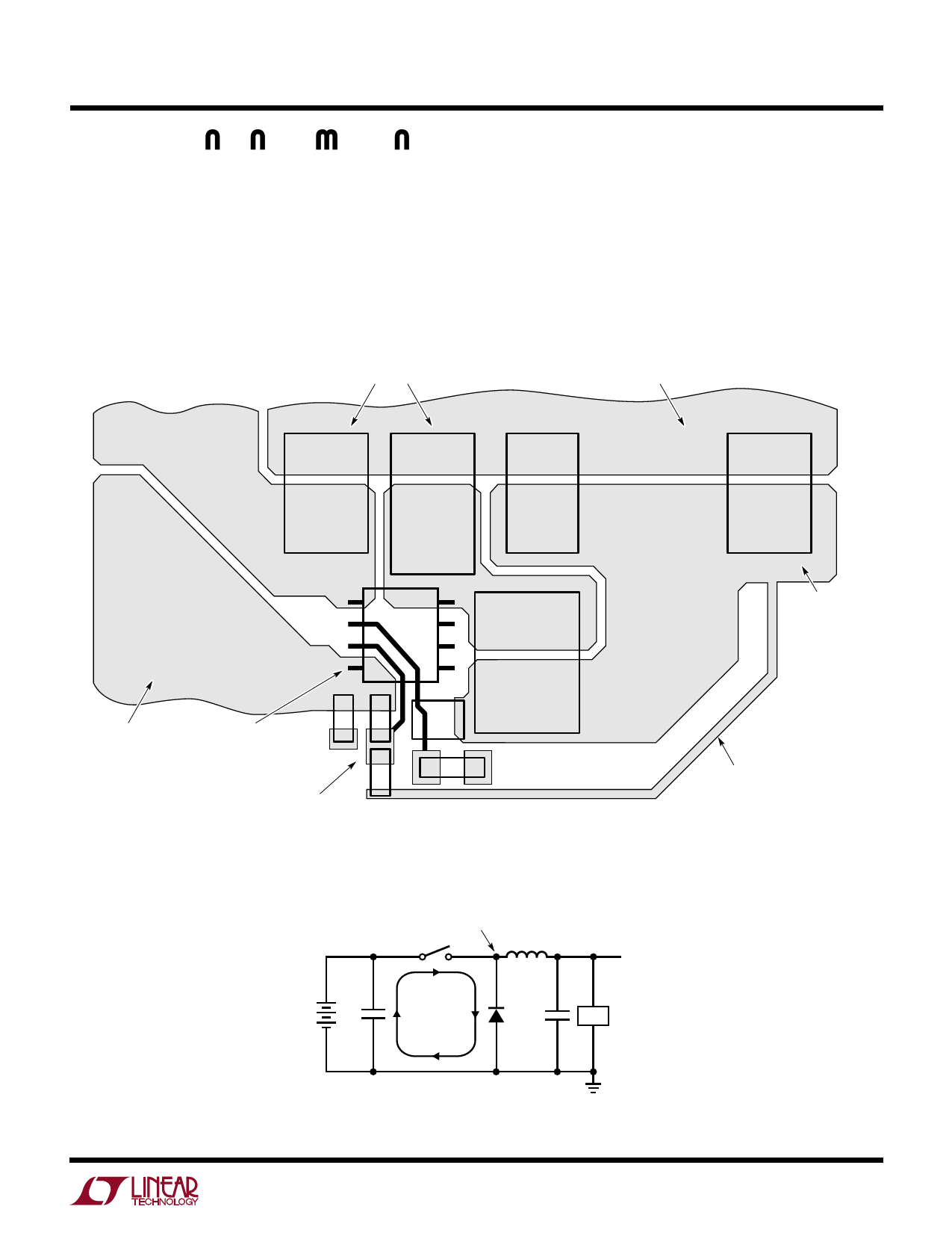
from the switch node. Also note that the high current
ground path of the catch diode and input capacitor are kept
very short and separate from the analog ground line.
The high speed switching current path is shown schemati-
cally in Figure 6. Minimum lead length in this path is
essential to ensure clean switching and low EMI. The path
including the switch, catch diode, and input capacitor is
the only one containing nanosecond rise and fall times. If
you follow this path on the PC layout, you will see that it is
irreducibly short. If you move the diode or input capacitor
away from the LT1506, get your resumé in order. The
other paths contain only some combination of DC and
500kHz triwave, so are much less critical.
MINIMIZE LT1506 C3, D1 LOOP
CONNECT TO
GROUND PLANE
VIN
C3
D1
C5
GND
C6
1
GND
U1
L1
VOUT
TAKE OUTPUT
DIRECTLY FROM
END OF OUTPUT
CAPACITOR
C1 R3
CONNECT TO
PLACE FEEDTHROUGHS
GROUND PLANE AROUND GND PIN FOR GOOD
THERMAL CONDUCTIVITY
R2
KEEP FB AND VC COMPONENTS
AWAY FROM HIGH FREQUENCY,
HIGH CURRENT COMPONENTS
D2
C4
Figure 5. Suggested Layout (Topside Only Shown)
KELVIN SENSE
VOUT
1506 F05
SWITCH NODE
L1
5V
HIGH
FREQUENCY
VIN
CIRCULATING
PATH
LOAD
1506 F06
Figure 6. High Speed Switching Path
15
Share Link: 