LT3467 查看數據表(PDF) - Linear Technology
零件编号
产品描述 (功能)
生产厂家
LT3467 Datasheet PDF : 18 Pages
| |||
LT3467/LT3467A
APPLICATIONS INFORMATION
Compensation—Theory
Like all other current mode switching regulators, the
LT3467/LT3467A needs to be compensated for stable
and efficient operation. Two feedback loops are used in
the LT3467/LT3467A: a fast current loop which does not
require compensation, and a slower voltage loop which
does. Standard Bode plot analysis can be used to under-
stand and adjust the voltage feedback loop.
As with any feedback loop, identifying the gain and phase
contribution of the various elements in the loop is critical.
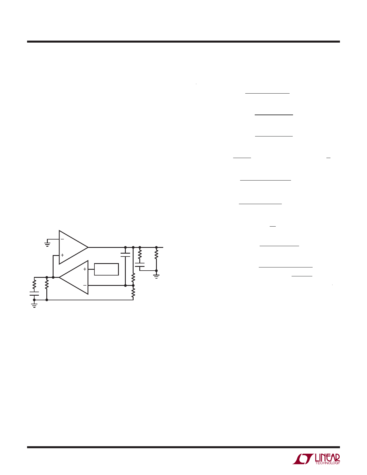
Figure 6 shows the key equivalent elements of a boost
converter. Because of the fast current control loop, the
power stage of the IC, inductor and diode have been re-
placed by the equivalent transconductance amplifier gmp.
gmp acts as a current source where the output current is
proportional to the VC voltage. Note that the maximum
output current of gmp is finite due to the current limit
in the IC.
–
gmp
+
VOUT
CPL
RESR RL
VC
RC RO
1.255V
REFERENCE
gma
COUT
R1
CC
R2
3467 F06
CC: COMPENSATION CAPACITOR
COUT: OUTPUT CAPACITOR
CPL: PHASE LEAD CAPACITOR
gma: TRANSCONDUCTANCE AMPLIFIER INSIDE IC
gmp: POWER STAGE TRANSCONDUCTANCE AMPLIFIER
RC: COMPENSATION RESISTOR
RL: OUTPUT RESISTANCE DEFINED AS VOUT DIVIDED BY ILOAD(MAX)
RO: OUTPUT RESISTANCE OF gma
R1, R2: FEEDBACK RESISTOR DIVIDER NETWORK
RESR: OUTPUT CAPACITOR ESR
Figure 6. Boost Converter Equivalent Model
From Figure 6, the DC gain, poles and zeroes can be
calculated as follows:
Output
Pole:
P1=
2
•
π
•
2
RL
•
COUT
Error Amp Pole: P2=
1
2 • π • RO • CC
Error
Amp
Zero:
Z1=
2
•
π
•
1
RC
•
CC
DC
GAIN:
A=
1.255
VOUT 2
•
VIN
• gma
• RO
• gmp
• RL
•
1
2
ESR
Zero:
Z2
=
2
•
π
•
1
RESR
•
COUT
RHP
Zero:
Z3=
2
•
VIN2 • RL
π • VOUT2
•
L
High Frequency Pole: P3> fS
3
Phase
Lead
Zero
:
Z4
=
2
•
π
•
1
R1•
CPL
Phase
Lead
Pole
:
P4
=
2
•
π
•
1
CPL •
R1• R2
R1+ R2
The current mode zero is a right-half plane zero which can
be an issue in feedback control design, but is manageable
with proper external component selection.
3467afe
10
Share Link: 