MAX3088CSA 查看數據表(PDF) - Maxim Integrated
零件编号
产品描述 (功能)
生产厂家
MAX3088CSA
Maxim Integrated

MAX3088CSA Datasheet PDF : 20 Pages
| |||
Fail-Safe, High-Speed (10Mbps),
Slew-Rate-Limited RS-485/RS-422 Transceivers
Detailed Description
The MAX3080–MAX3089 high-speed transceivers for
RS-485/RS-422 communication contain one driver and
one receiver. These devices feature fail-safe circuitry,
which guarantees a logic-high receiver output when the
receiver inputs are open or shorted, or when they are
connected to a terminated transmission line with all
drivers disabled (see Fail-Safe section). The MAX3080/
MAX3081/MAX3082 feature reduced slew-rate drivers
that minimize EMI and reduce reflections caused by
improperly terminated cables, allowing error-free data
transmission up to 115kbps (see Reduced EMI and
Reflections section). The MAX3083/MAX3084/MAX3085
offer higher driver output slew-rate limits, allowing
transmit speeds up to 500kbps. The MAX3086/
MAX3087/MAX3088’s driver slew rates are not limited,
making transmit speeds up to 10Mbps possible. The
MAX3089’s slew rate is selectable between 115kbps,
500kbps, and 10Mbps by driving a selector pin with a
three-state driver.
The MAX3082/MAX3085/MAX3088 are half-duplex
transceivers, while the MAX3080/MAX3081/MAX3083/
MAX3084/MAX3086/MAX3087 are full-duplex trans-
ceivers. The MAX3089 is selectable between half- and
full-duplex communication by driving a selector pin
high or low, respectively.
All of these parts operate from a single +5V supply.
Drivers are output short-circuit current limited. Thermal
shutdown circuitry protects drivers against excessive
power dissipation. When activated, the thermal shut-
down circuitry places the driver outputs into a high-
impedance state.
Receiver Input Filtering
The receivers of the MAX3080–MAX3085, and the
MAX3089 when operating in 115kbps or 500kbps
mode, incorporate input filtering in addition to input
hysteresis. This filtering enhances noise immunity with
differential signals that have very slow rise and fall
times. Receiver propagation delay increases by 20%
due to this filtering.
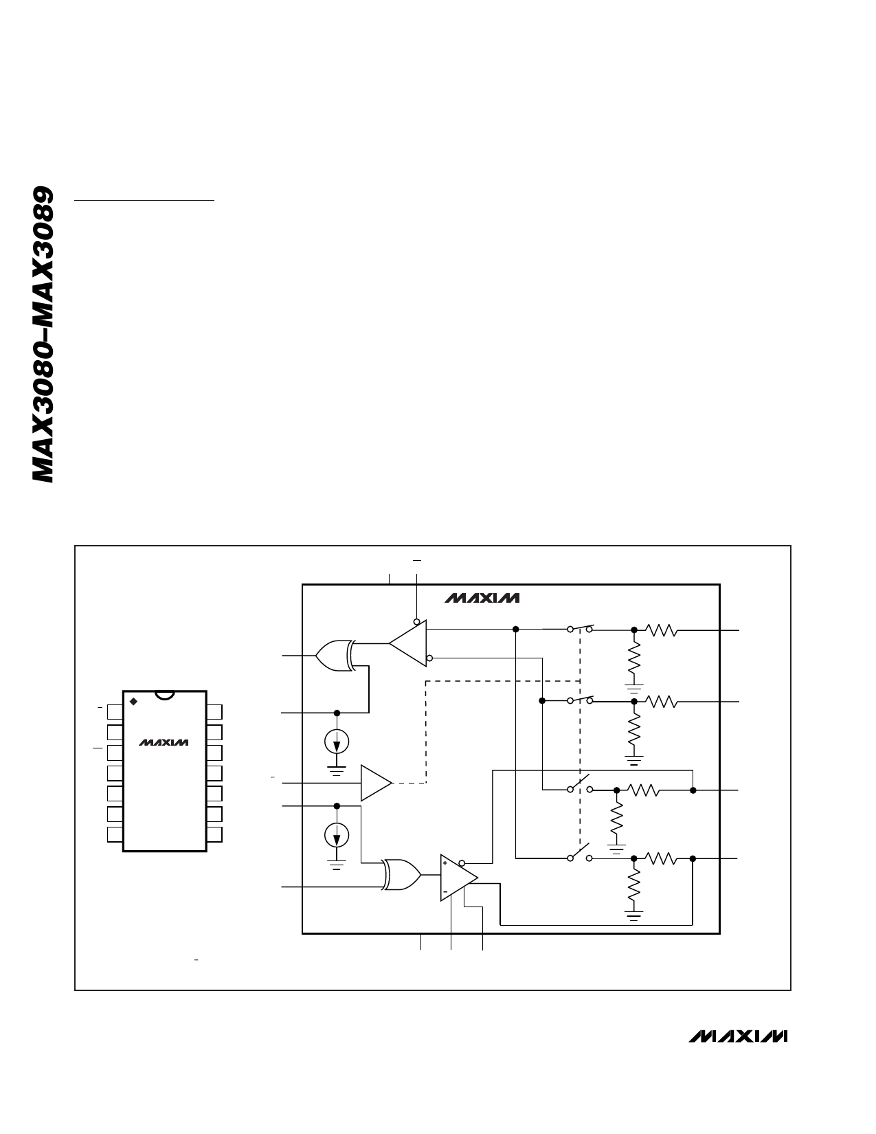
VCC RE
MAX3089
A
RD
TOP VIEW
B
H/F 1
14 VCC
RO 2
13 RXP
RE 3 MAX3089 12 A
DE 4
11 B
H/F
DI 5
10 Z
Z
SRL 6
TXP
9Y
GND 7
8 TXP
DIP/SO
Y
DI
NOTE: SWITCH POSITIONS
INDICATED FOR H/F = GND
GND DE SRL
Figure 4. MAX3089 Pin Configuration and Functional Diagram
14 ______________________________________________________________________________________
Share Link: