MAX8568A 查看數據表(PDF) - Maxim Integrated
零件编号
产品描述 (功能)
生产厂家
MAX8568A Datasheet PDF : 17 Pages
| |||
Complete Backup-Management ICs
for Lithium and NiMH Batteries
Pullup resistors, R3 and R4 in Figure 7, should be select-
ed to ensure that when OD1 and OD2 go high imped-
ance, the gate of the external MOSFET discharges within
50µs to 100µs. This time allows the backup converters to
start and provide power to I/O and MEM. Discharges
longer than 50µs to 100µs could cause the main supply
to back drain current from the MAX8568 and allow the
I/O OUT and MEM OUT voltage to droop. The MOSFET
gate-source resistor, RGS, is calculated from the follow-
ing formulas:
τ = RGS x CISS
τ=
−50µs
ln 1 −
VGS(TH)
VBKSU
where the MOSFET gate-source threshold, VGS(TH),
and MOSFET input capacitance, CISS, are provided on
the MOSFET data sheet.
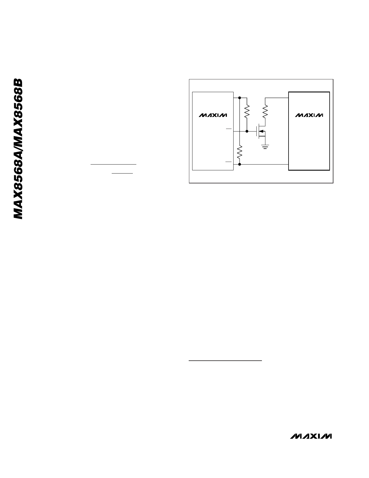
Connection with MAX1586
When the MAX8568 is used with the MAX1586 system
power supply, it may be preferable to employ the
MAX1586’s voltage monitors to determine when backup
should start. The connection for this is shown in Figure 5
where the dead-battery output (DBO) of the MAX1586
drives the INOK input of the MAX8568. This, in effect,
overrides the voltage-sensing circuit on the MAX8568
and uses the DBO monitor on the MAX1586. Refer to the
MAX1586 data sheet for information on how to set the
DBO threshold. The CHG connection in Figure 5 is
described in the next section.
Terminating Charging at a Voltage Other
than the Switchover Voltage
In normal operation, the MAX8568 charger is always
active as long as the INOK voltage is valid (above
2.43V). In some systems, however, it may be desirable to
terminate backup battery charging when the main bat-
tery is somewhat depleted but not so low as to trigger
backup. An external voltage monitor, or a voltage moni-
tor in a power-supply IC, such as the MAX1586, can dis-
able charging by disconnecting the CHGI resistor. If
CHGI is open, no charging current flows. This can be
accomplished with the circuit in Figure 5. The low-battery
output (LBO) of the MAX1586 pulls low when the battery
falls below a user-set level (refer to the MAX1586 data
sheet). This turns off the external n-channel MOSFET (or
IN
MAX1586
LBO
DBO
CHGI
1MΩ
RCHGI
n-CHANNEL
MOSFET OR
OPEN-DRAIN
INVERTER
MAX8568
1MΩ
INOK
Figure 5. Using a MAX1586 Power-Supply IC to Trigger
Backup Switchover and to Disable Backup Battery Charging
Prior to Switchover
open-drain logic inverter) and disconnects the current
path through RICHG. Backup charging can be stopped
for any reason using this method.
PC Board Layout and Routing
Careful PC board layout is important for minimizing
ground bounce and noise. Ensure that C1 (IN input
capacitor), C2 (BK input capacitor), C3 (BKSU bypass
capacitor), and C4 (LDO output capacitor) are as close
as possible to the IC. Avoid using vias to connect C2 or
C3 to their respective pins or GND. C2 and C3 grounds
should be next to each other, and this connection can
then be used as the star ground point. All other grounds
should connect to the star ground. PGND should star at
C2 and C3, and should not connect directly to the
exposed pad (EP) of the MAX8568. Connect EP to the
bottom layer ground plane, and then connect the
ground plane to the star ground. Vias on the inductor
path are acceptable if necessary. IN, BK, BKSU, and
LDO traces should be as wide as possible to minimize
inductance. Refer to the MAX8568 evaluation kit for a
PC board layout example.
Chip Information
TRANSISTOR COUNT: 7902
PROCESS: BiCMOS
14 ______________________________________________________________________________________
Share Link: 