MB89935B 查看數據表(PDF) - Fujitsu
零件编号
产品描述 (功能)
生产厂家
MB89935B Datasheet PDF : 42 Pages
| |||
MB89930A Series
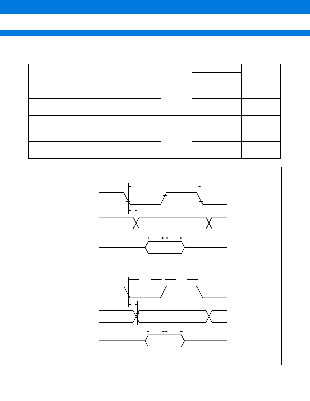
(7) UART, Serial I/O Timing
(VCC = 5.0 V ± 10%, AVSS = VSS = 0.0 V, Ta = −40 °C to +85 °C)
Parameter
Symbol Pin name Condition
Value
Min
Max
Unit Remarks
Serial clock cycle time
tSCYC
UCK/SCK
2 tINST*
µs
UCK/SCK ↓ → SO time
Valid SI → UCK/SCK↑
tSLOV UCK/SCK, SO Internal shift −200
200 ns
tIVSH UCK/SCK, SI clock mode 1/2 tINST*
µs
UCK/SCK ↑ → Valid SI hold time tSHIX UCK/SCK, SI
1/2 tINST*
µs
Serial clock “H” pulse width
tSHSL
UCK/SCK
tINST*
µs
Serial clock “L” pulse width
UCK/SCK ↓ → SO time
Valid SI → UCK/SCK
tSLSH
UCK/SCK
External
tINST*
µs
tSLOV UCK/SCK, SO shift clock
0
200 ns
tIVSH UCK/SCK, SI
mode
1/2 tINST*
µs
UCK/SCK ↑ → Valid SI hold time tSHIX UCK/SCK, SI
1/2 tINST*
µs
* : For information on tinst, see “ (4) Instruction Cycle”.
• Internal Shift Clock Mode
UCK/SCK
SO
SI
tSCYC
0.8 V
2.4 V
tSLOV
2.4 V
0.8 V
tIVSH
tSHIX
0.8 VCC 0.8 VCC
0.2 VCC 0.2 VCC
0.8 V
• External Shift Clock Mode
UCK/SCK
0.2 VCC
SO
SI
tSLSH
tSHSL
0.2 VCC
0.8 VCC
tSLOV
2.4 V
0.8 V
tIVSH
tSHIX
0.8 VCC 0.8 VCC
0.2 VCC 0.2 VCC
0.8 VCC
31
Share Link: 