MCP23017T-ESO 查看數據表(PDF) - Microchip Technology
零件编号
产品描述 (功能)
生产厂家
MCP23017T-ESO Datasheet PDF : 42 Pages
| |||
MCP23017/MCP23S17
3.5.3
INTERRUPT-ON-CHANGE
CONTROL REGISTER
The GPINTEN register controls the
interrupt-on-change feature for each pin.
If a bit is set, the corresponding pin is enabled for
interrupt-on-change. The DEFVAL and INTCON
registers must also be configured if any pins are
enabled for interrupt-on-change.
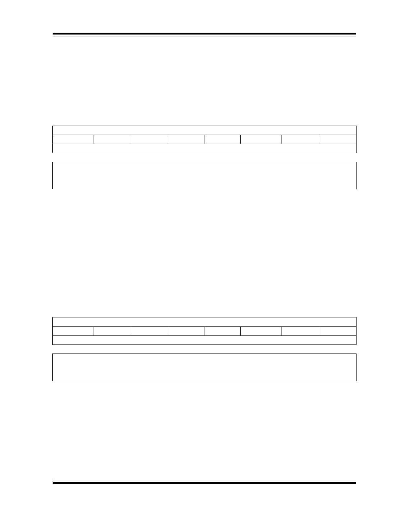
REGISTER 3-3: GPINTEN: INTERRUPT-ON-CHANGE PINS (ADDR 0x02) (Note 1)
R/W-0
GPINT7
bit 7
R/W-0
GPINT6
R/W-0
GPINT5
R/W-0
GPINT4
R/W-0
GPINT3
R/W-0
GPINT2
R/W-0
GPINT1
R/W-0
GPINT0
bit 0
Legend:
R = Readable bit
-n = Value at POR
W = Writable bit
‘1’ = Bit is set
U = Unimplemented bit, read as ‘0’
‘0’ = Bit is cleared
x = Bit is unknown
bit 7-0
GPINT<7:0>: General purpose I/O interrupt-on-change bits <7:0>
1 = Enables GPIO input pin for interrupt-on-change event.
0 = Disables GPIO input pin for interrupt-on-change event.
Note 1: Refer to INTCON.
3.5.4
DEFAULT COMPARE REGISTER
FOR INTERRUPT-ON-CHANGE
The default comparison value is configured in the
DEFVAL register. If enabled (via GPINTEN and
INTCON) to compare against the DEFVAL register, an
opposite value on the associated pin will cause an
interrupt to occur.
REGISTER 3-4: DEFVAL: DEFAULT VALUE REGISTER (ADDR 0x03)
R/W-0
DEF7
bit 7
R/W-0
DEF6
R/W-0
DEF5
R/W-0
DEF4
R/W-0
DEF3
R/W-0
DEF2
R/W-0
DEF1
R/W-0
DEF0
bit 0
Legend:
R = Readable bit
-n = Value at POR
W = Writable bit
‘1’ = Bit is set
U = Unimplemented bit, read as ‘0’
‘0’ = Bit is cleared
x = Bit is unknown
bit 7-0
DEF<7:0>: Sets the compare value for pins configured for interrupt-on-change from defaults <7:0>
(Note 1)
If the associated pin level is the opposite from the register bit, an interrupt occurs. (Note 2)
Note 1: Refer to INTCON.
2: Refer to INTCON and GPINTEN.
2005-2016 Microchip Technology Inc.
DS20001952C-page 19
Share Link: 