AD7818AR 查看數據表(PDF) - Analog Devices
零件编号
产品描述 (功能)
生产厂家
AD7818AR Datasheet PDF : 20 Pages
| |||
AD7816/AD7817/AD7818
For example, if the result of a conversion on Channel 0 was
1000000000 (512 Dec), the ambient temperature is equal to
–103°C + (512/4) = +25°C.
Table II below shows some ADC codes for various temperatures.
Table II. Temperature Sensor Output
ADC Code
00 1100 0000
01 0011 1000
01 1001 1100
10 0000 0000
10 0111 1000
11 1001 0000
Temperature
–55°C
–25°C
0°C
+25°C
+55°C
+125°C
TEMPERATURE MEASUREMENT ERROR DUE TO
REFERENCE ERROR
The AD7816, AD7817, and AD7818 are trimmed using a pre-
cision 2.5 V reference to give the transfer function described
previously. To show the effect of the reference tolerance on a
temperature reading, the temperature sensor transfer function
can be rewritten as a function of the reference voltage and the
temperature.
CODE (Dec) = ([113.3285 × K × T]/[q × VREF] – 0.6646) × 1024
where:
K = Boltzmann’s Constant, 1.38 × 10⁻²³
q = Charge on an electron, 1.6 × 10⁻¹⁹
T = Temperature (K)
So, for example, to calculate the ADC code at 25°C
CODE = ([113.3285 × 298 × 1.38 × 10–23]/[1.6 × 10–19 × 2.5]
– 0.6646) × 1024
= 511.5 (200 Hex)
As can be seen from the expression, a reference error will pro-
duce a gain error. This means that the temperature measure-
ment error due to reference error will be greater at higher
temperatures. For example, with a reference error of –1%, the
measurement error at –55°C would be 2.2 LSBs (0.5°C) and
16 LSBs (4°C) at 125°C.
SELF-HEATING CONSIDERATIONS
The AD7817 and AD7818 have an analog-to-digital conversion
function capable of a throughput rate of 100 kSPS. At this
throughput rate the AD7817 and AD7818 will consume between
4 mW and 6.5 mW of power. Because a thermal impedance is
associated with the IC package, the temperature of the die will
rise as a result of this power dissipation. The graphs below show
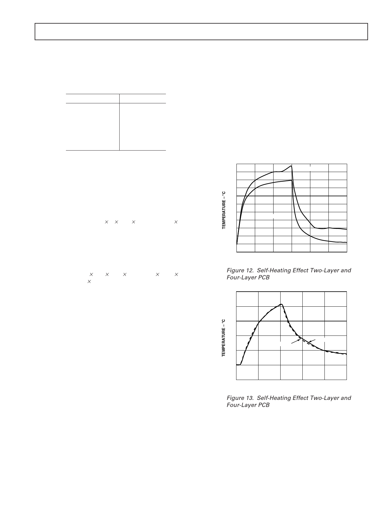
the self-heating effect in a 16-lead SOIC package. Figures 12
and 13 show the self-heating effect on a two-layer and four-layer
PCB. The plots were generated by assembling a heater (resistor)
and temperature sensor (diode) in the package being evaluated.
In Figure 12, the heater (6 mW) is turned off after 30 sec. The
PCB has little influence on the self-heating over the first few
seconds after the heater is turned on. This can be more clearly
seen in Figure 13 where the heater is switched off after 2 sec-
onds. Figure 14 shows the relative effects of self-heating in air,
fluid and in thermal contact with a large heat sink.
These diagrams represent the worst-case effects of self-heating.
The heater delivered 6 mW to the interior of the package in all
cases. This power level is equivalent to the ADC continuously
converting at 100 kSPS. The effects of the self-heating can be
reduced at lower ADC throughput rates by operating on Mode
2 (see Operating Modes section). When operating in this mode,
the on-chip power dissipation reduces dramatically and, as a
consequence, the self-heating effects.
0.50
2-LAYER PCB
0.45
0.40
0.35
0.30
0.25
0.20
4-LAYER PCB
0.15
0.10
0.05
0.00
–0.05
0
10
20
30
40
50
60
TIME – secs
Figure 12. Self-Heating Effect Two-Layer and
Four-Layer PCB
0.25
0.20
0.15
0.10
2-LAYER PCB
4-LAYER PCB
0.05
0.00
–0.05
0
1
2
3
4
5
TIME – secs
Figure 13. Self-Heating Effect Two-Layer and
Four-Layer PCB
REV. C
–13–
Share Link: 