MTD9N10E1(2005) 查看數據表(PDF) - ON Semiconductor
零件编号
产品描述 (功能)
生产厂家
MTD9N10E1 Datasheet PDF : 12 Pages
| |||
MTD9N10E
Preferred Device
Power MOSFET
9 Amps, 100 Volts
N−Channel DPAK
This advanced Power MOSFET is designed to withstand high
energy in the avalanche and commutation modes. The new energy
efficient design also offers a drain−to−source diode with a fast
recovery time. Designed for low voltage, high speed switching
applications in power supplies, converters and PWM motor controls,
these devices are particularly well suited for bridge circuits where
diode speed and commutating safe operating areas are critical and
offer additional safety margin against unexpected voltage transients.
• Avalanche Energy Specified
• Source−to−Drain Diode Recovery Time Comparable to a
Discrete Fast Recovery Diode
• Diode is Characterized for Use in Bridge Circuits
• IDSS and VDS(on) Specified at Elevated Temperature
• Replaces MTD6N10
MAXIMUM RATINGS (TC = 25°C unless otherwise noted)
Rating
Symbol Value
Drain−Source Voltage
Drain−Gate Voltage (RGS = 1.0 MΩ)
Gate−Source Voltage
− Continuous
− Non−Repetitive (tp ≤ 10 ms)
Drain Current − Continuous
Drain Current − Continuous @ 100°C
Drain Current − Single Pulse (tp ≤ 10 µs)
Total Power Dissipation
Derate above 25°C
Total Power Dissipation @ TA = 25°C, when
mounted to minimum recommended pad
size
VDSS
VDGR
VGS
VGSM
ID
ID
IDM
PD
100
100
± 20
± 30
9.0
5.0
27
40
0.32
1.75
Operating and Storage Temperature
Range
TJ, Tstg
−55 to
150
Single Pulse Drain−to−Source Avalanche
EAS
40
Energy − Starting TJ = 25°C
(VDD = 25 Vdc, VGS = 10 Vdc,
IL = 9.0 Apk, L = 1.0 mH, RG = 25 Ω)
Thermal Resistance
− Junction to Case
− Junction to Ambient
− Junction to Ambient, when mounted
to minimum recommended pad size
RθJC
RθJA
RθJA
3.13
100
71.4
Maximum Temperature for Soldering
Purposes, 1/8″ from case for 10
seconds
TL
260
Unit
Vdc
Vdc
Vdc
Vpk
Adc
Apk
Watts
W/°C
Watts
°C
mJ
°C/W
°C
http://onsemi.com
9 AMPERES
100 VOLTS
RDS(on) = 250 mΩ
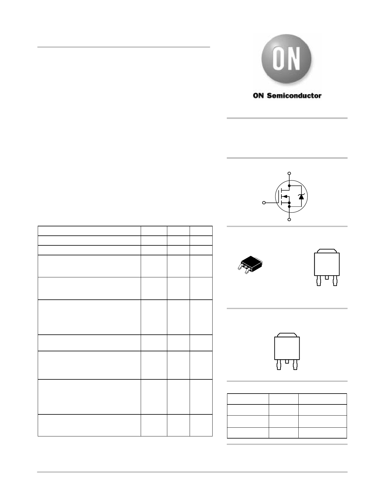
N−Channel
D
G
S
MARKING
DIAGRAM
4
12
3
Y
WW
T9
CASE 369A
DPAK
STYLE 2
= Year
= Work Week
= MOSFET
YWW
T9
N10E
PIN ASSIGNMENT
4
Drain
1 23
Gate Drain Source
ORDERING INFORMATION
Device
Package
Shipping
MTD9N10E
DPAK
75 Units/Rail
MTD9N10E1
DPAK
75 Units/Rail
MTD9N10ET4
DPAK 2500 Tape & Reel
Preferred devices are recommended choices for future use
and best overall value.
© Semiconductor Components Industries, LLC, 2005
1
February, 2005 − Rev. XXX
Publication Order Number:
MTD9N10E/D
Share Link: 