NCP4629 查看數據表(PDF) - ON Semiconductor
零件编号
产品描述 (功能)
生产厂家
NCP4629 Datasheet PDF : 15 Pages
| |||
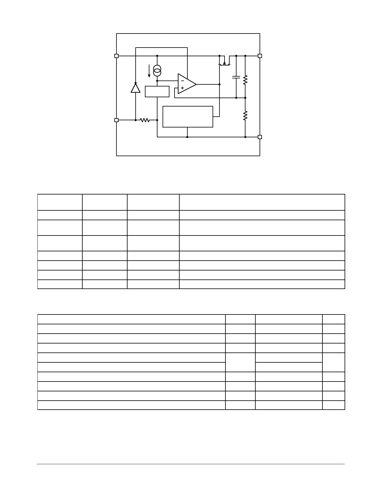
NCP4629
VIN
VOUT
Vref
Current Limit
CE
Short Protection
Thermal Shutdown
GND
Figure 2. Simplified Schematic Block Diagram
PIN FUNCTION DESCRIPTION
Pin No.
SOT−89
Pin No.
DPAK
Pin Name
Description
1
1
VIN
Input pin
2
2
GND*
Ground pin, all ground pins must be connected together when it is
mounted on board
3
3
GND*
Ground pin, all ground pins must be connected together when it is
mounted on board
4
4
CE
Chip enable pin (“H” active)
5
5
VOUT
Output pin
6
GND
Heatsink surface is internally connected to Pin 2 − GND
6
GND
Heatsink surface is internally connected to Pin 3 − GND
*Pin no.2 − GND and pin no.3 − GND of SOT−89 and DPAK−5 packages must be wired to the GND line when it is mounted on board.
ABSOLUTE MAXIMUM RATINGS
Rating
Symbol
Value
Unit
Input Voltage
Output Voltage
VIN
−0.3 to 36
V
VOUT
−0.3 to VIN ≤ 36
V
Chip Enable Input
VCE
−0.3 to VIN ≤ 36
V
Power Dissipation SOT−89−5
Power Dissipation DPAK−5
PD
900
mW
1900
Junction Temperature
TJ
−40 to 150
°C
Storage Temperature
TSTG
−55 to 125
°C
ESD Capability, Human Body Model (Note 2)
ESDHBM
2000
V
ESD Capability, Machine Model (Note 2)
ESDMM
200
V
Stresses exceeding Maximum Ratings may damage the device. Maximum Ratings are stress ratings only. Functional operation above the
Recommended Operating Conditions is not implied. Extended exposure to stresses above the Recommended Operating Conditions may affect
device reliability.
1. Duration time = 200 ms
2. This device series incorporates ESD protection and is tested by the following methods:
ESD Human Body Model tested per AEC−Q100−002 (EIA/JESD22−A114)
ESD Machine Model tested per AEC−Q100−003 (EIA/JESD22−A115)
Latch−up Current Maximum Rating tested per JEDEC standard: JESD78.
http://onsemi.com
2
Share Link: 